


 English (pdf)
 Article in xml format
 Article references
 Send this article by e-mail
 Cited by SciELO
  Cited by Google
  Similars in
SciELO
Similars in
SciELO  Similars in Google
 Permalink
1. Introduction
The development of power semiconductors based on materials with wide forbidden band like Silicon Carbide (SiC) has become a viable alternative to replace the actual Silicon power devices due to its advantages like: wider forbidden band (2x), higher electrons speed saturation (2x) and better thermal conductivity (5x). These advantages help to avoid the use of heatsinks improving switching frequency and reducing the switching losses with better stability against temperature [1-4]. The Power-MOS based on (SiC) is one of the devices ready to replace the actual Power-MOS silicon solution mainly in applications with high temperature and high current density like power converters.
The electrical characteristics of the SiC-Mosfet require an early fault detection subsystem to isolate any fault as fast as possible avoiding the damage of the components and protecting the application. In literature have been reported different fault detection techniques based on the measurement of the collector voltage, collector current, gate voltage and the induced voltage from the inductance of the emitter wire for IGBTs [5-9]. However, the implementation of a fault detection circuit represents a higher cost with complex configurations and low performance for fault detection and reverses voltage transients. Other reported techniques are based on the measurement of the voltage level changes [10], deviation of the normalized current [11,12], and the voltage slew rate [13,14]. These techniques are faster than those previous mentioned. However, to find the fault several measurements are necessary causing a late detection of the fault due to the complex analysis even in steady state and only for open-circuit fault condition.
In [15-17] have been showed that a correct analysis of the gate signal (IGBT Mosfet) allows a microseconds detection time. To apply a technique based on the gate behavior of the SiC-Mosfet is necessary to analyze the charge behavior of the internal capacitances C GS and C GD due to the small capacitance value (1900 pF) and the gate charge less than 28 nC for 1200V@25A [18].
In this paper is presented a novel fault detection technique based on the analysis of the SiC-Mosfet gate while is turning-on. Simulation and experimental results are shown for a boost topology. The theoretical analysis of the gate charge is included with simulation results of the fault detection system proposed and the experimental results to validate the proposal.
2. Analysis of V GS behavior when is turning-on
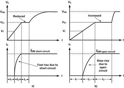
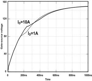
In Figure 1 is showed the analytical behavior of the gate-source voltage and its dependency with the drain current for a non-fault condition. Due to the interaction between the SiC Mosfet and the external circuitry it is necessary to consider the kind of load [19]. The analysis of the load is showed in Figure 2 where V T is the threshold voltage, V G1 is the flat phase voltage and V GM is the maximum applied voltage to the converter. Each period of time represent a phase of V GS respecting I D . The initial conditions for the analysis are: V GS =0, I D =0 and V DS =V DD .
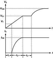

2.1 Period t 1
V GS depends of the charge C GS +C GD through R G , while it rises from zero to the activation level V T , I D is 0A. This period of time is defined as turn-on delay and the behavior is given by (1).
2.2 Period t 2
V GS >V T this condition sets the current through the drain and is proportional to the gate voltage with a g m slew rate. Due to the Miller effect in the capacitance C GD the charge has an exponential behavior according with (2).
2.3 Period t 3
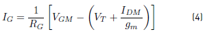
I D has its maximum level given by the external load connected to the Mosfet. Because I D is constant the gate voltage is constant (flat phase) which is given by (3).
Because V GS is constant, all the current flows through the capacitance C GD , at the same time V D decreases near zero which forces the gate current to follow the charge of C GD (4).
After period t 3 , C GD is still charged forcing V GS to rise exponentially to the maximum value V GM .
From the presented behavior is observed the dependency of I D with respect to V GS during t 3 (flat phase). As can be seen on (3), if I D changes (short-circuit or open circuit fault) a change on V GS is induced. In Figure 3 is presented the theoretical behavior caused by short-circuit and open circuit fault condition.
3. Simulation results when V GS is turning-on
In order to select the appropriate thresholds during the flat phase of V GS , the behavior of the SiC-Mosfet was simulated with different values of I D and R G for short-circuit and open-circuit faults.
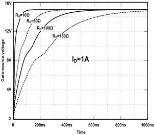
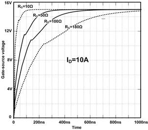
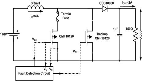
The device used was the CMF10120 (I D =10A, V DS =1200V) from Cree Company.
In Figures 4 and 5 is showed the behavior of V GS for I D =1A and 10A with R G variations. For R G =10Ω the dynamic of the C GD charge is incremented and the time of the flat phase is reduced. With R G =180Ω the dynamic of the C GD charge is reduced and the time of the flat phase is increased. In Figure 6 is showed the comparative of V GS for I D =1A and 10A with R G =180Ω. From these results was concluded that R G =180Ω allows an optimal dynamic of the V GS charge for an appropriate experimental measurement with short-circuit and open-circuit fault conditions.
4. Fault detection system
Figure 7 shows the block diagram of the fault detection system based on [16,17]. It is formed by a differential block, window voltage comparator, hysteresis comparator, ramp generator, zones comparator and the decision circuit.
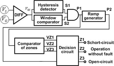
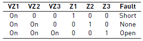
The zones comparator works according with Table 1. For a non-fault condition only VZ1 and VZ2 thresholds are working. When a short-circuit fault occurs VZ1 is activated and when an open-circuit fault occurs VZ1, VZ2 and VZ3 are activated.
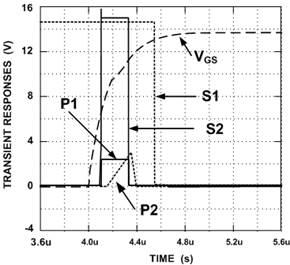
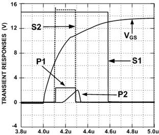
In Figure 8 simulation results are presented for a non-fault condition where the following responses are shown: differential circuit V GS , hysteresis circuit S1, window comparator S2, logic multiplier circuit P1=S1*S2 and ramp generator P2 as function of the pulse width P1. In Figure 9 are showed the thresholds levels VZ1 and VZ2.
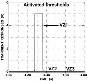
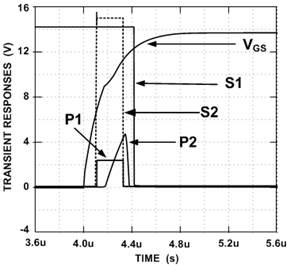
In Figure 10 are showed the simulation results for a short-circuit fault condition where can be seen that signal P2 has smaller amplitude due to the flat phase time reduction according with the drain current increment. In Figure 11 is showed the corresponding VZ1 threshold level.
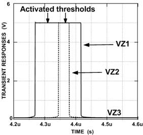
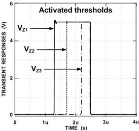
In Figure 12 are showed the simulation results for an open-circuit fault condition where can be seen that signal P2 has a bigger amplitude due to the flat phase time increment according with the increment of I D . In Figure 13 are showed the corresponding threshold levels VZ1, VZ2 y VZ3.
5. Experimental results
In order to validate the fault detection circuit a boost converter was designed with the following characteristics: I out =2A, ∆V 0=3V, F SW =50 kHz and ∆I IND =1.2A [20]. The circuit to detect, isolate and replace the damaged component is presented in Figure 14. On it is observed the replacement SiC-Mosfet which is activated immediately when the proposed fault detection system detects a fault condition.
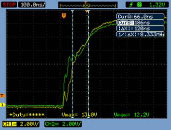
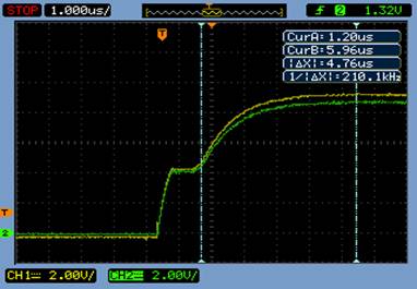
In Figures 15, 16 and 17 are showed the signals V GS of the differential block for a non-failure condition, short-circuit failure and open-circuit failure. The yellow waveform is the gate signal of the SiC-Mosfet and the green waveform is the acquired signal from the instrumentation amplifier. From the waveforms is possible to verify the theoretical influence of the flat phase time, for a short-circuit failure condition the duration of the phase is reduce and for open-circuit failure condition the duration of the phase is incremented.
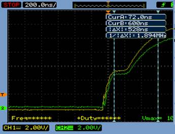
In Figures 18, 19 and 20 are showed the experimental results for the logic multiplier and the ramp generator for a non-fault condition, short-circuit fault and open-circuit fault. The green waveform is P1 and the yellow waveform is P2.
It is possible to see that the ramp amplitude is reduced when a short-circuit fault condition occurs and is incremented when an open-circuit fault occurs. This behavior is according with the simulation results from Figures 8, 10 and 12.
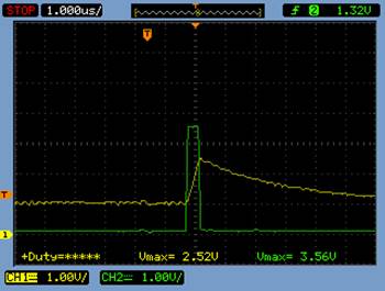
Figure 18 Experimental results of the logic multiplier and the ramp generator for a non-fault condition
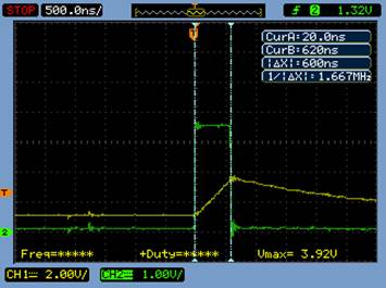
Figure 19 Experimental results of the logic multiplier and the ramp generator for a short-circuit fault condition
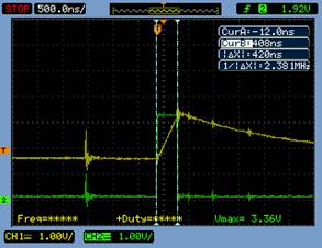
Figure 20 Experimental results of the logic multiplier and the ramp generator for an open-circuit fault condition
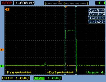
In Figures 21, 22 and 23 are showed the experimental results of the decision block for: non fault, short-circuit fault and open-circuit fault conditions. Green waveform is the digital signal Z2 and yellow waveform is the digital signal Z1. This behavior corresponds with the description on Table 1.
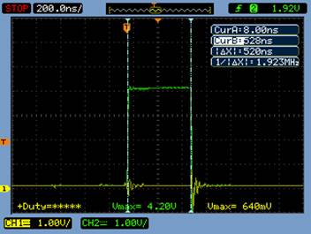
Figure 21 Experimental results when Z2 is activated from the decision block for a non-fault condition
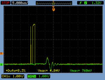
Figure 22 Experimental results when Z3 and Z2 are activated from the decision block for an open-circuit fault condition
6. Conclusions
In this paper has been presented simulation and experimental results for an early fault detection system applied for a SiC-Mosfet. The objective was to obtain early fault detection for a high dynamic system like the SiC-Mosfet on a switching power supply. In order to validate the system, the gate signal was analyzed for different fault conditions (non-fault, short-circuit fault and open circuit fault). According with the results the fault was mitigated making use of a replacement component to avoid the propagation of the fault. Future work includes the incorporation of the thresholds making use of an adaptive algorithm to improve the robustness of the proposed system.

