


 English (pdf)
 Article in xml format
 Article references
 Send this article by e-mail
 Cited by SciELO
  Cited by Google
  Similars in
SciELO
Similars in
SciELO  Similars in Google
 Permalink
Introduction
Plasma Electrolytic Oxidation (PEO) has been reported in the fabrication of ceramic-type coatings on metals such as aluminum, titanium, magnesium, and alloys in order to increase their resistance to exposure and wear, improving their tribological properties 1,2. In the particular case of titanium, this technique has been used for surface modification with the aim of obtaining the oxide of this metal, widely studied for its wide bandgap of forbidden energy, which makes it a good candidate for photocatalyst for pollutant charge reduction 3. However, to guarantee the viability of this process at an industrial scale, it is important to explore the PEO with other metals, such as Zn, Cu, and stainless steel, costing $3.78 4, $9.59 5 and $5 6 per kilogram, respectively, which are cheaper than titanium ($34.75) 7. This study presents the results of Cr(VI) photoreduction using the coatings over these metallic substrates.
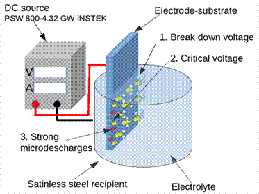
In some variations of conventional PEO, the substrate-electrode acts as the anode (anodic PEO), and the electrolyte container vessel or a platinum electrode is the cathode 8; these methods include power supplies with variable or switchable output voltage at a given frequency and duty cycle 9. This methodology allows control of the grain size of the oxide, directly formed on the substrate surface. Unlike conventional anodizing, in which low electrical voltages are used for exposure times longer than 20 min, the PEO involves the use of high magnitude voltages for less time.
The PEO consists of the surface modification of a metal that is immersed in an electrolyte solution contained in a metallic container. The concentration of the electrolyte determines the current intensity that flows through the substrate while it is subjected to an electrical voltage higher than the breakdown voltage of the material. When the breakdown voltage is exceeded, microdischarges are generated on the surface of the sample; thereby, the local pressure and temperature abruptly increase, producing microcavities. The current density can be controlled by considering the substrate shape and the applied electric potential 10.
Several processes use hexavalent chromium (Cr(VI)) to manufacture some products; in the automotive industry, one of them is electroplating or deposition of a metallic layer of chromium on objects to add reflective brightness and provide corrosion protection 11; in the manufacture of paint and pigments, Cr(VI) is added to the product to improve its stability 12, and in the tannery, it is used to transform the collagen in the leather into a stable material to prevent its degradation and to increase its useful life 13,14. The Cr quantity that is not deposited, impregnated or absorbed in these techniques is returned to the environment through wastewater. This is harmful to health 15,17, so it is necessary to reduce Cr(VI) to Cr(III), which is less toxic and more environmentally friendly.
Although other reduction processes of hexavalent to trivalent chromium are currently used, such as bioremediation and chemical reactors 18-20, the fixation of materials for advanced oxidation presents advantages, such as the reuse of the catalyst, without complex recovery or addition of toxic agents.
The use of the cathodic configuration has been reported for PEO on certain metals and alloys; in this configuration, the substrate is placed as the cathode and the container vessel, or another electrode, as the anode 21. Thus, several authors have modified stainless steel surfaces decreasing the electric potential and low concentrations of the electrolyte 22. In this work, the PEO anodic configuration was used with copper and zinc substrates, and the cathodic mode with the steel substrates. Based on the results, the existence of the corresponding oxides on each substrate and their efficiency in Cr(VI) photoreduction was probed; which do not have been reported before, in the best of our knowledge; most of the reports are related to oxide samples in powder for this application.
Materials and methods
Sheets of dimensions 20 mm x 20 mm x 1 mm of stainless steel (304), copper (Cu-DHP 1/2 hard CW024A) and zinc (shiny sheet EN 988) were previously polished with an abrasive paper and used as substrates. Before the PEO, these metal sheets were subjected to an ultrasonic bath for 20 min with distilled water and isopropanol. In all cases, the exposure time was 10 min, and a mixture of 0.2 g/L sodium metasilicate nonahydrate (Na2SiO3-9H2O) and 0.05 g/L potassium hydroxide (KOH) was utilized as electrolyte.
The PEO of copper and zinc substrates was carried out by conventional mode with potential differences between the electrodes of 450, 550, 650 and 750 V, while the surface of stainless-steel substrates was modified with PEO cathodic configuration, applying 350, 450, and 550 V. In all cases, an INSTEK PSW 800-4.32 GW source was used by constant voltage mode. A schematic of the experimental setup for the PEO in anodic configuration is shown in the schema of Figure 1, in which the positive of the source was connected to the substrate-electrode and the negative to the metal vessel. In the cathodic arrangement, the polarity of the source leads was reversed.
The X-ray diffractograms (XRD) of the samples were obtained with the grazing angle method, using an XBruker D8-Advance equipment, with a scan between 20° and 90°, at 5 s per degree, an operating voltage of 40 kV and current of 8 mA. The average crystalline size (S) of the coatings was estimated from XRD patterns, according to the Scherrer equation (Equation (1)) 23:
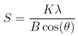
Where B is the full width at half maximum (FWHM) in radian, corresponding to the most intense diffraction peak; K = 0.9 is the shape factor or Scherrer constant; λ is the X-ray wavelength of CuKα radiation (1.54056 Å) and θ is the Bragg’s diffraction angle.
The contributions of the crystallite size and lattice strain to diffraction peak broadening were calculated by the Williamson-Hall (WH) method, using Equation 2 24:
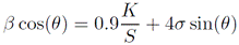
Where β is the measured FWHM of XRD, corresponding to different crystal planes, and σ is the effective strain.
The porous formation, cracks, and agglomerations during the growing of oxide layers could increase the surface-volume ratio, which has a direct influence on the photocatalytic activity. For this reason, in the present work, images of the coatings were taken with a JEOL JSM-5900LV Scanning Electron Microscope (SEM) to observe the sample surface morphology.
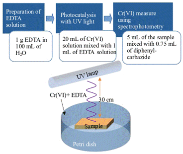
The physicochemical process of photoreduction involves the in situ generation of active radical species, especially hydroxyls, which lead to the destruction of pollutant targets. Therefore, a photocatalytic agent is used under the action of light in the presence of substances containing OH groups such as EDTA (ethylenediaminetetraacetic acid). A schema of the photocatalysis method is shown in Figure 2.
The photocatalytic activity was evaluated by irradiating the films, immersed in a solution of Cr(VI)-EDTA, with ultraviolet light of wavelength 255 nm from a 15 W bactericidal lamp. The complete reduction efficiency was obtained after 60 minutes. The test was performed in a climatic chamber, controlling the temperature to around 23 °C.
The standard method ASTM-3500 B-Cr 25 was applied to calculate the removal rate (R), using a spectrophotometer (EU-2800DS) to measure the absorbance of the sample solutions under the maximum absorbance wavelength (352 nm). Considering the direct relationship between concentration and absorbance, the R of Cr(VI) in the solution was calculated through Equation 3:

Where C 0 and C f are the initial and final Cr(VI) concentration, expressed in mg/L.
The kinetic model of the photocatalytic reaction, using the simplification to first-order that assumes isothermal conditions, can be expressed as follows (Equation (4)) <26:
Where, C is the concentration at the time t and k r is the rate constant of degradation.
In the experiments, three concentrations during the treatment of Cr(VI) aqueous solution were measured, so the analysis of experimental data was carried out with three points for the fit-linear process, using Equation (4). Although this number of points is low, the obtained values of the rate constant of degradation were only considered as estimations for comparison purposes; although the behavior of these experimental points clearly showed a decrease of C/C 0 in the function of the exposition time, more data could be necessary to guarantee this information.
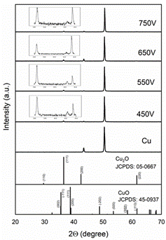
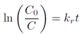
Figure 3 Diffractograms of copper substrates, modified by PEO with voltages between 450 and 750 V. In each case, the inserted plot corresponds to a magnification between 36 and 44°
Results
Coatings of Cu2O over Cu substrates
The diffractograms of the coatings of Cu substrate-electrode obtained with each PEO potential difference are shown in Figure 3. In the case of the pure copper substrate, two peaks were presented around 43.5° and 50.5°, which is similar to that reported by Theivasanthi and Alagar 27. On the other hand, four low- intensity peaks around 29.66°, 36.53°, 42.44° and 61.57° are observed, related to the (110), (111), (200) and (220) crystallographic directions of cuprous oxide (Cu2O) (JCPDS: 05-0667), after surface modification by PEO 28,29. In any case, the formation of cupric oxide (CuO) was observed.
In Figure 4, the WH plots were made for all the observed diffraction peaks; the sin(θ) values along the x-axis and β cos(θ) values along the y-axis were drawn. The intercept with the y-axis of the best linear-fitting is related to the nanocrystalline size (S), and the slope gives the lattice strain multiplicated by four (4 σ). In Table 1, the corresponding values were registered. The S values obtained by Scherrer and WH methods are different due to the distribution of particle sizes in the sample 30. It is possible to note that the size grain decreases while PEO voltage increases. On the other hand, the strain has a proportional behavior to this growth parameter, which suggests an increase in the dislocation density caused by this rising voltage.
The SEM micrograph of the 550 V-treated substrate, shown in Figure 5, indicates a surface modification with irregular topography of a flak-like shape.
The use of copper (I) and (II) oxides in the degradation of organic pollutants has been reported by other authors 31,32; these p-type semiconductors have a narrow bandgap of 1.2-1.8 eV and 2.0-2.2 eV, respectively, which allows their photoactivity with UV and visible light.
The photocatalytic activity of the Cu2O coatings in the photoreduction of Cr(VI)-EDTA was evaluated through the data plotted in Figure 6. It can be seen a reduction rate close to 100 % within 60 min with the samples, although with the coating grown at 450 V, the highest efficiency was achieved at 30 min of the process.
The k r values were obtained from the slope of the linearly fitted plot in Figure 6 c) by using Equation (4), and the data were registered in Table 2. It is possible to see that the highest k r value was obtained with the coating grown at 650 V PEO.
Coatings of ZnO over Zn substrates
The diffractograms in Figure 7 correspond to the PEO-modified zinc substrates. It can be observed the formation of zinc oxide related to the broad bands around 31.80, 34.47, 36.29, 47.60, 56.65, 62.94, 66.45, 68.03, and 69.16° (JCPDS: 036-1451), by which the intensity augmented as a function of increasing voltage. This is in agreement with those reported by other authors 33,34.
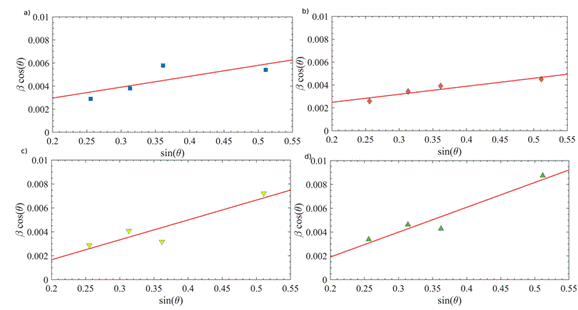
Figure 4 WH analysis corresponding to diffractograms in Figure 3 of Cu2O coatings grown by PEO with voltages between a) 450, b) 550, c) 650, and d) 750 V. The continuous line represents the best linear-fitting for calculus of grain size of nanocrystals and strain effect
Figure 5 SEM micrograph of PEO-modified copper substrate at an electrical potential 550. The behavior was similar in the other samples
In the experiments, once the plasma is obtained on the substrate surface, the current tends to be a constant value, but the electrolyte evaporates rapidly due to the high temperature reached, leading to the partial uncovering of the substrate-electrode. The band gap energy of this semiconductor material has been reported to be between 3.2 and 3.5 eV at room temperature 35,36.
Table 2 The rate constant of degradation corresponding to analysis in Figure 6 c) of degradation of Cr(VI)-EDTA with the Cu2O coating samples. R² is the R-square statistic of the linear fitting
| Sample | k r (min-1) | R² |
|---|---|---|
| 450V | 0.02 | 0.988 |
| 550V | 0.02 | 0.999 |
| 650V | 0.03 | 0.988 |
| 750V | 0.02 | 0.995 |
| Cu | 0.001 | 0.999 |
Table 3 Grain sizes (S) of the ZnO coatings
| Sample | Scherrer S (nm) | W-H S (nm) | σ |
|---|---|---|---|
| 450V | 27.16 | 20.12 | 0.0094 |
| 550V | 10.75 | 7.92 | -0.0053 |
| 650V | 16.57 | 31.08 | 0.0044 |
| 750V | 9 | 6.09 | -0.0060 |
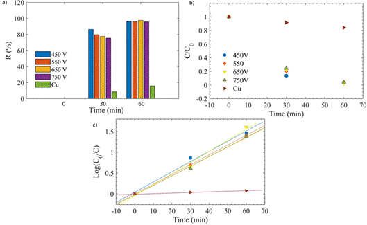
Figure 6 a) R (%), b) C/C 0 and c) log (C 0 /C) of the photocatalytic process of the Cu2O samples in the reduction of Cr(VI)-EDTA as a function of the exposition time. In this last plot, the solid line represents the best linear fitting

Table 4 The rate constant of degradation corresponding to the analysis in Figure 10 c) of degradation of Cr(VI)-EDTA with the ZnO coating samples
| Sample | k r (min-1) | R² |
|---|---|---|
| 450V | 0.05 | 0.92 |
| 550V | 0.05 | 0.93 |
| 650V | 0.05 | 0.95 |
| 750V | 0.05 | 0.96 |
| Zn | 0.01 | 0.99 |
The WH plots were made for all the observed diffraction peaks, as can be seen in Figure 8. The intercept with the y-axis of the best linear-fitting is related to S and from the slope of the best-fit line was estimated σ. In Table 3, the corresponding values were registered. As mentioned before, the difference between S values obtained by Scherrer and WH methods is associated with the distribution of particle sizes in the sample 26. Taking into account the plots in Figure 8 b) and Figure 8 d), it is possible to note that the grain size for the 650 V sample is out of the behavior of rising while PEO voltage increases. This can be caused by negative strain, due to the lattice shrinkage, for the ZnO-NPs obtained with 550 V and 750 V at PEO.
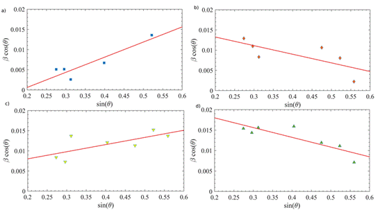
Figure 8 WH analysis corresponding to the diffractograms of PEO-modified zinc substrates using a) 450, b) 550 V, c) 650 V, and d) 750 V
A SEM micrograph of the zinc substrate modified by PEO at 550 V is shown in Figure 9. In this case, the accumulation of irregular grains of different sizes and shapes distributed over the entire surface of the coating can be observed, which shows internal porosity and a sponge-like structure.
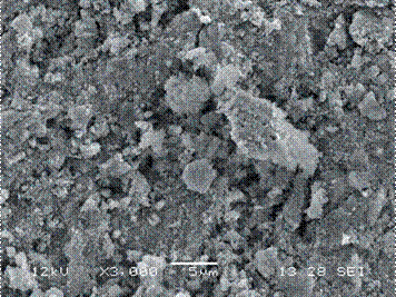
Figure 9 SEM surface morphology of the ZnO sample, obtained by PEO with an electrical potential of 550 V. The behavior of the surface modification was similar using the other voltages
The photocatalytic performance of the ZnO coatings was tested in the reduction of Cr(VI)-EDTA with an initial concentration of 1 ppm. The reduction rates as a function of time are presented in Figure 10, showing a behavior similar to that described above for the Cu2O coatings, reaching a reduction of around 100 % within 60 min. The highest efficiency was achieved at 30 min with the samples obtained by PEO, using 650 and 750 V.
The k r values, obtained from the slope of the linearly fitted plot in Figure 10 c) by using Equation (4), were registered in Table 4. It is possible to see that k r was the same for all ZnO coatings.
3.3 Coatings of Fe2O3 and Fe3O4 over stainless steel substrates
Substrate-electrodes of stainless steel 304 were treated by PEO, and its modified surface was analyzed to search for the growth of iron oxides, known as Hematite (Fe2O3) and Magnetite (Fe3O4). These compounds have been reported in advanced oxidation process applications for textile industry wastewater treatment and as antibacterial for general purposes 37-39. In Figure 11, the plotted diffractograms correspond to the coatings that were prepared by cathodic PEO, using 350, 450 and 550 V between the electrodes; the diffraction peaks were associated with the (2 0 2), (3 0 0) and (0 2 10) crystallographic planes of Fe2O3 (JCPDS: 330664); (6 2 2) of Fe3O4 (JCPDS 190629) and (2 0 0) of γ-Fe (ICCD 98-004-1506). This intensity changed for the samples according to the surface modification of the steel sheet by cathodic PEO 40-41.
Table 5 Grain sizes (S) of Fe2O3 and Fe3O4 coatings on stainless steel 304 substrates
| Sample | Scherrer (Fe3O4) S (nm) | Scherrer (Fe2O3) S (nm) | W-H S (nm) | σ |
|---|---|---|---|---|
| 350V | 17.28 | 21.45 | 10.49 | -0.0034 |
| 450V | 26.04 | 38.98 | 18.85 | 0.0070 |
| 550V | 21.94 | 39.43 | 25.96 | 0.0054 |
In Figure 12, the WH plots were made for all the observed diffraction peaks corresponding to Fe2O3. The intercept with the y-axis of the best linear-fitting is related to S and from the slope was estimated σ. In Table 5, the corresponding values were registered. The S values obtained by Scherrer and WH methods for both Fe2O3 and Fe3O4 are different, due to the distribution of particle sizes in the sample 26. It is possible to note that the grain size increases while PEO voltage rises. On the other hand, the strain was negative for the lowest voltage and the strain minimum was obtained with the highest voltage.
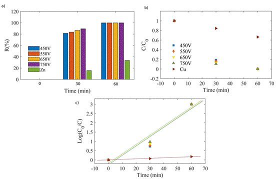
Figure 10 Photocatalytic efficiency of Cr(VI)-EDTA reduction with PEO-modified zinc sheets at electric potentials of 450, 550, 650, and 750 V
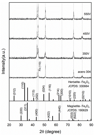
Figure 11 Diffractograms of PEO-modified 304 stainless steel substrates with inter-electrode voltages of 350, 450, and 550 V
From Figure 13, two SEM micrographs of the surface of the steel substrate modified by PEO at 550 V can be observed. The formation of crater-like pores and spheroidal nodules over the coating is observed, which increases the surface area, enhancing its photocatalytic activity. This morphology is different from that obtained by other authors, using cathodic PEO with a pulsed DC power supply; for instance, Jin et al. reported a surface in some hill-shaped embossment, employing voltages low 280 V 42, while Wu et al., found a rough surface with some granular bulges under 400 V 43. This behavior is as expected, because the effects of spark discharges can be mitigated by the application of pulsed current, providing control over the impact of plasma discharge on the surface 44.
Table 6 The rate constant of degradation corresponding to analysis in Figure 14 c) of degradation of Cr(VI)-EDTA with Fe2O3 and Fe3O4 coating samples
| Sample | k r (min-1) | R² |
|---|---|---|
| 350V | 0.02 | 0.92 |
| 450V | 0.02 | 0.94 |
| 550V | 0.03 | 0.88 |
| steel | 0 | 0.995 |
In Figure 14, the reduction behavior of Cr(VI)-EDTA using the PEO-modified stainless steel sheets is shown. A complete reduction was found within 60 min, using the samples obtained at 550 and 650 V. The k r values obtained from the slope of the linearly fitted plot in Figure 14 c) by using Equation (4) were registered in Table 6. It is possible to see that the highest k r value was achieved with the coating grown at 550 V during the PEO.
The obtained coatings had a morphology that depended on the type of substrate. For the copper, the flak-like shape structures over the surface were grown, while for zinc substrate-electrodes, it can be seen agglomerations of the zinc oxide have a sponge-like appearance. In contrast, stainless steel crater-like microcavities, and spheroidal nodules were generated over its surface. This may be related to the fact that this material contains other elements such as chromium, manganese, and nickel, apart from iron and carbon; thus, other types of bonds can be produced on the surface of the substrate, and the topography of the substrate changes 45.
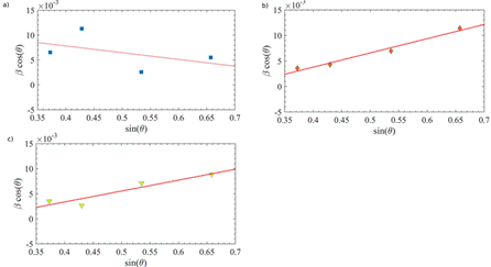
Figure 12 WH analysis corresponding to the diffractograms of PEO-modified stainless steel substrates using a) 350, b) 450 V, and c) 550 V.
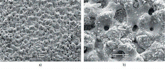
Figure 13 SEM micrographs of the surface of stainless-steel substrate modified by PEO with 550 V, using a magnification of a) X1000 and b) X5000
The high-energy processes, such as the PEO, promote the formation of new compounds that cannot be obtained by conventional chemical or physical methods 46. Particularly for soft metals, the melting point plays an important role; this temperature for copper is 1357.77 K, while for zinc is 692.68 K, so the modification of surfaces by PEO with different characteristics in both such cases is expected.
According to the estimated values of k r , the highest photocatalytic efficiency of Cr(VI) reduction was achieved using the ZnO coatings, possibly due to the wide bandgap of this semiconductor. However, the size grain did not have an influence in these results.
To compare the obtained results about reduction of Cr(VI) to Cr(III) with the reports of other authors, it was necessary to consider nanoparticle photocatalysts because corresponding studies with pure oxide coatings were not found. In this way, for example, with ZnO nanoparticles prepared by co-precipitation method with an average size of 20-50 nm, the photocatalytic ability of Cr(VI) reduction was 90% under UV-light irradiation for 17 h with and k r = 0.025 min-1 (47, while in the present work, this value was doubled.
On the other hand, with Cu2O, the corresponding reduction rate of Cr(VI) was k r =0.00294 min−1, under visible light irradiation, according to Xincheng-Dou et al48, which is a value 90% less than that reported in this work, but using UV-light radiation.
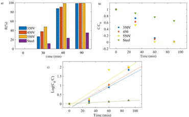
Figure 14 Cr(VI)-EDTA reduction rate with PEO-modified stainless steel sheets at voltages of 350, 450, and 550 V
Liu TY et al. reported that k r ranged from 0.0072 min-1 to 0.0304 min-1, using dosages between 0.5 and 3 g/L of Fe2O3 nanoparticles 49; while pure Fe3O4 nanoparticles hardly reduced Cr(VI) within 90 min under visible light irradiation with a value of k r =0.008 cm-1, as reported by Ting-Ge et al.50. In contrast, in this work, with coatings containing both Fe3O4 and Fe2O3, a k r =0.03 min -1was found, a similar value to that maximum reported by Liu TY et al.
Conclusions
The PEO modification of the surfaces of the copper, zinc, and stainless-steel substrates was obtained by varying the voltage between the electrodes. The formation of layers of Cu2O, ZnO and Fe2O3 and Fe3O4, over each corresponding material, was verified by X-ray diffraction. As a growth parameter, this differential of potential affected the crystalline structure of the coatings since the intensity and width of the peaks changed in the related diffractograms. On the other hand, according to the micrographs of the surface of the samples, the morphology of the coating depends on the current demand and the characteristics of the power supply to support the output voltage.
The lattice strain factor had an important role in the formation of the nanocrystalline Cu2O coatings; this was evidenced in the differences between estimated sizes with Scherrer and WH methods. Using the sample grown to 650 V, the rate of degradation of Cr(VI) was slightly higher than those obtained with the others coatings on the Cu substrates. On the other hand, the strain factor had a low influence on the generation of ZnO, Fe2O3, and Fe3O4 nanostructures, which can be inferred from the minor alteration of the grain size, calculated with both models, Scherrer and WH. While the rate of degradation with the coatings containing Fe2O3 and Fe3O4 was similar to that obtained with Cu2O, the highest value of this parameter was achieved using the ZnO coatings.
Using ultraviolet radiation over the samples, the total photoreduction of Cr(VI)-EDTA was obtained within 60 minutes. For this reason, these coatings have the potential for use in the treatment of chromium-containing wastewater. In particular, PEO-treated stainless steel can be the best candidate, due to its high porosity corresponding to uniformly distributed microcavities.

