


 English (pdf)
 Article in xml format
 Article references
 Send this article by e-mail
 Cited by SciELO
  Cited by Google
  Similars in
SciELO
Similars in
SciELO  Similars in Google
 Permalink
1 Introduction
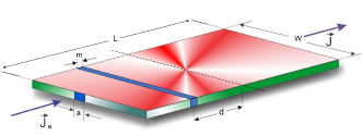
The resistive superconducting state of a mesoscopic sample in presence of a transport current can be explained by the well know kinematic vortex-anti-vortex (v-Av) pair. This v-Av pair is considered as propagating waves of the order parameter ψ, in which, the electronic superconducting density nearly vanishes along the line where kinematic vortices move [1, 2, 3, 4, 5, 6, 7, 8, 9, 10, 11]. Sivakov et al experimentally found that the V-Av pairs move with velocity ukv ≃ 105 m/s, while that the Abrikosov vortices velocity is uav ≃ 103 m/s. Due to their high velocity, kinematic vortices resemble a line where the order parameter is deprecated [1, 2, 4]. Several theoretical research in superconducting films in presence of external currents has been carried out in the last years, i.e., Sardella et al showed that an external current can active magnetically the kinematic vortices in a superconducting square with a central hole. Also, they found that the superconducting electronic density alongside the slip phase line has crucial importance to describe the maximum of the current-resistance curve [12, 13, 14, 15]. Berdiyorov et al studied the kinematic vortex state on the time response of a bridge with pinning in presence of an applied current. They show that the resistive state is characterized by the possible vortex states and depends strongly on the external current, also studied the kinematic state in samples with magnetic dots, finding that dots increase the interval of currents for which a resistive state occurs, where a change in the phase θ of π, is the responsible of this kinematic vortex [5, 6, 7, 8, 16]. An analysis of the superconducting electronic density at the border of the sample was studied by Benfenati et al, they found that due to the inter-band coupling effect in a two-band system exist a difference between the critical temperature in the bulk and the surface, also, the presence of the border (boundary) induce strong variations of the gaps with the presence of several length scales [17]. Also, several experimental works in superconductrs and semi-conductor materials have been carried out, for example, structural analysis, surface morphology, magnetic ordering, dielectric response and optical characteristic in a complex perovskite Dy 2 BiFeO 6 , clay mineral Illite, Chlorite, Hematite was studied, they found that the reflectance curve as a function of wavelength reveals the typical behavior of a double perovskite-type semiconductor. Also the electrical properties of the clay showed a strong non-linear insulating behavior [18, 19]. Also, the influence of the rugosity of the sample on the critical currents and the kinematic vortex velocity was studied in the references [20, 21, 22]. In this work, we study the resistive response of the superconducting film with a non-centered transversal channel under an applied current at zero magnetic field (see Figure 1). A study was carried out by considering different widths of the channel, distance of the center of the film, and sizes of the metallic contact in which the external current is applied. We found that the value of the critical current density, at which the first kinematic vortex enters the sample J 1, and the superconducting-normal state transition current J 2 , strongly depends on these parameters. This paper is outlined as follows. In Section 2 we describe the theoretical formalism used to study a mesoscopic film n the presence of an applied current at zero magnetic field. In Section 3 we present the results that come out from the numerical solution of the Ginzburg-Landau equations, finally, in Section 4 we present our conclusions.
2 Theoretical Formalism
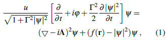
The studied sample is a thin superconducting film of length L and width w; the width of the contacts through which a constant current density Ja is applied is a. We treated this system as a 2D system [23, 24, 25]. The general form of the time-dependent General Ginzburg Landau equations (G-TDGL) in dimensionless units is given by [26, 27, 28]:
And
The function f (r) = 1 for all regions except in the channel were we choose f (r) = 0 simulating a thermal defect at lower critical temperature Tc or a metallic channel. The heating effects are not taken into accout [29, 30]. The electrostatic potential is Δϕ and is given in units of ϕ0 = ħ/2et GL , the distances are given in the coherence length ξ units, the time is in units of the Ginzburg-Landau time tGL = π ħ 8kBTcu, and the vector potential A is given in H c2 ξ , where Hc2 is the upper critical field. u = 5.79 and Γ = tEψ0/ħ = 10, t E is the inelastic scattering time [26]. ψ ≠ 0 is used in all the boundary of the sample, except at the metallic contact, where we used ψ = 0 and ∇ϕ |n= −Ja, where Ja is the external current in units of J0 = cσħ /2et GL , σ is normal electrical conductivity, and the mesh-grid size is δ =0.1 [2, 7, 13]). To solve the equation (1) and Equation (2), we used the popular link-variable method [31, 32, 33].
3 Results
In Figure 1, we illustrate the studied sample, a thin film with L = 12ξ, and w = 8ξ. The external dc current density J a is uniformly applied through the electrodes width a (a/ξ = 2,4,6,8).
In Figure 1, we show the analyzed sample, a thin film with L = 12ξ, and w = 8ξ. The external dc current density Ja is uniformly applied through the electrodes of width a (a/ξ = 2,4,6,8). A non-centered channel of depleted superconductivity of width m is present at a distance d of the center of the film. In the Figures 2 and 3, we plotted the time-averaged voltage V and the resistivity ∂V/∂ J a (right) as a function of the applied current Ja respectively, we use metallic contact of size a/ξ = 2,4,6,8. This figure shows a decreasing of the critical currents in which the vortex anti-vortex pair occurs in the sample, J 1 and J 2 by increasing a for a homogeneous sample and a slight dependence of a and d on these critical currents.
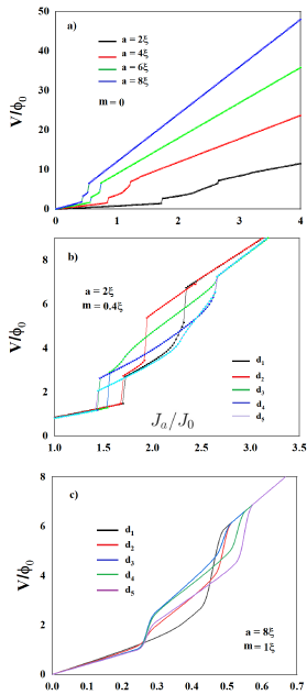
Figure 2 (Color online) Time-averaged voltage V as function of the applied current-density J a for a) Homogeneous sample with a/ξ = 2,4,6,8, (b) m = 0.4ξ, α = 2ξ and the channel positioned in d1 = 5.6%, d2 = 4.2ξ, d3 = 2.8ξ, d4 = 1.4ξ, d5 = 0 (as is evident this value simulates a centered channel), measured from the center of the sample, and c) m = 1ξ, a = 8 ξ and a channel positioned in d1 = 5.6ξ, d2 = 4.2ξ, d3 = 2.8ξ, d4 = 1.4ξ, d5 = 0.
In the Figure 2(b) and Figure 3(b), the same curve is plotted for m = 0.4ξ, a = 2ξ and the channel positioned in d1 = 5.6ξ, d2 = 4.2ξ, d3 = 2.8ξ, d4 = 1.4ξ, d5 = 0. Being d5 = 0 a centred channel. It would be expected that given the width of the metallic contact and the position of the channel, which generate different electronic densities that would favor the movement of Cooper pairs, increasing a and d has a strong influence on the creation of v - Av pairs. In addition, it is shown that the maximum of the peaks in the resistivity curve increase as a increases for a sample without a channel, but this maximum does not show any variation when taking a constant a and varying the channel distance d.
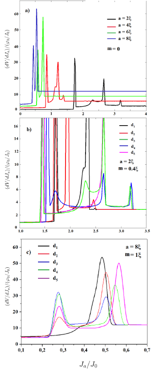
Figure 3 (Color online) Resistivity ∂V/∂J a , as function of the applied current-density J a for a) Homogeneous sample with a/ξ = 2,4,6,8, (b) m = 0.4ξ, a = 2ξ and the chanel positioned in d1 = 5.6ξ, d2 = 4.2ξ, d3 = 2.8ξ, d4 = 1.4ξ, d5 = 0 (as is evident this value simulates a centered channel), measured from the center of the sample, and c) m = 1ξ, a = 8ξ and a channel positioned in d1 = 5.6ξ, d2 = 4.2ξ, d3 = 2.8ξ, d4 = 1.4ξ, d5 = 0.
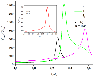
Figure 4 (Color online) Average velocity of the V-Av pairs for a = 2ξ, m = 0.4ξ and d1 = 5.6ξ, d4 = 1.4ξ, and d5 = 0. (Inset) a = 4ξ, m = 0.
In Figure 4, the velocity of a v - Av pair during the annihilation process (v - Av interaction) is plotted for α = 2ξ, m = 0.4 and d1 = 5.6ξ, d4 = 1.4ξ, and d 5 = 0. And for a homogeneous sample with α = 4ξ ,(Inset).
We note that the value of the current where the maximum of the velocity of the kinematic vortices diminishes as d decreases. So, due to the presence of the defect in the sample, the kinematic vortices movement is directly affected by the presence of the channel, and due to that, the interaction is due to the oscillations of the phonos of the crystalline network, which could be in out of phase, due to the difference of the electronic density of the v - Av pair. As we showed in the reference [22], the V - Av pairs are nucleated at the edge of the sample and annihilate each other at the center, in our system not is possible to appreciate this dynamic (Figure 5), maybe due to the size of the computational mesh. It is very interesting to note (Figures 5 (b,c)), that when the channel is at a distance d4 = 1.4ξ, and only for this case, and considering J = J1, the kinematic vortices are created in a line perpendicular to the current applied in that position. Quite the contrary of the other cases, when J ≠ J 1 is considered, this line is created in the center of the sample. In a previous work [22], we studied the resistive state of a superconducting strip with an engineered centered defect at different Tc. We found that the asymmetry induced by the defect affects the current distribution in the sample and the V-Av pair enters at the sample, not through the central line. We think that due to the small width of the channel m, only when the channel is located at d4 does it have an asymmetric current distribution that affects the central entry point. In Figure 6, we plot the relationship between J1 (J2 and the width of the metallic contact a. As can be seen, J1 and J2 decrease with a. J1 = 1.75 for a = 2ξ, J1 = 0.82 for a = 4ξ, J1 = 0.59 for a = 6ξ and J1 = 0.46 for a = 8ξ, also, J2 = 2.69 for a = 2ξ, J2 = 1.24 for a = 4ξ, J2 = 0.74 for a = 6ξ and J1 = 0.52 for a = 8ξ. The decrease of J1 and J2 means that for higher a, will be necessary to apply a small current to reach the normal state, it its due to the less diamagnetic the material will be. So the appearance of a resistive state occurs for smaller J1 as a increases.
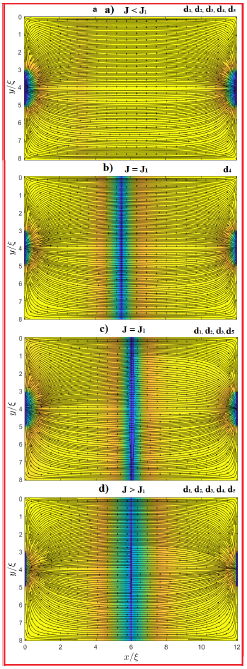
Figure 5 (Color online) Snapshots of the logarithm of the order parameter, ln|ψ | (yellow/blue corresponds to largest/zero | ψ |) for a) J < J1 for all d; J = J1 for b) d4, c) d1, d2, d3, d5 and d) J > J1 for all d.

4 Conclusions
By solving the time-dependent Ginzburg-Landau equations, we studied the superconducting state of a mesoscopic thin film under a transport electric current at a zero magnetic field. A non-centered channel of depleted superconductivity is present in the sample. We vary the width of the metallic contact in which the external current is applied. The numerical solutions of the time-dependent Ginzburg-Landau equations show that critical currents diminished as the size of the metallic contact increases, also, the value of current where the maximum of the velocity of annihilation of the kinematic vortices occurs grows as the distance of the channel at the center to the sample increases. Finally the resistive state in stripes can be controlled by a pulsed current, in case of stroboscopic resonances with the induced v-av motion.

