


Services on Demand
Journal
Article
 English (pdf)
 Article in xml format
 Article references
 Send this article by e-mail
Indicators
-
 Cited by SciELO
 -
 Access statistics
Related links
-
 Cited by Google
 -
 Similars in
SciELO
Similars in
SciELO -
 Similars in Google
Share

 Permalink
DYNA
Print version ISSN 0012-7353On-line version ISSN 2346-2183
Dyna rev.fac.nac.minas vol.78 no.166 Medellín Apr./June 2011
AN IMPROVED MEASUREMENT STRATEGY BASED ON STATISTICAL DESIGN OF EXPERIMENTS FOR A BOOST CONVERTER
ESTRATEGIA DE MEDICION MEJORADA BASADA EN DISEÑO ESTADISTICO DE EXPERIMENTOS PARA UN CONVERTIDOR ELEVADOR
HIRAM MORALES
Centro Nacional de Investigación y Desarrollo Tecnológico, Cuernavaca, Morelos, México, peabraha@cenidet.edu.mx
ABRAHAM CLAUDIO
Centro Nacional de Investigación y Desarrollo Tecnológico, Cuernavaca, Morelos, México, peabraha@cenidet.edu.mx
JESUS AGUAYO
Centro Nacional de Investigación y Desarrollo Tecnológico, Cuernavaca, Morelos, México, jaguayo@cenidet.edu.mx
MANUEL ADAM
Centro Nacional de Investigación y Desarrollo Tecnológico, Cuernavaca, Morelos, México, adam@cenidet.edu.mx
JESUS MINA
Centro Nacional de Investigación y Desarrollo Tecnológico, Cuernavaca, Morelos, México, jmina@cenidet.edu.mx
Received for review September 23th, 2009, accepted November 7th, 2010, final version November, 8th, 2010
ABSTRACT: This work presents a measurement strategy based on the statistical design of experiments to analyze the switching and conduction losses of the switches of a boost converter. The measurement strategy considers the measurement errors compensation and the reduction of sensors, but achieving a good quality and accuracy of the directly developed measurements. A very detailed analysis of the phenomena and parasitic elements of the circuit, which produce incorrect measurements of the variables of interest, is performed. Some recommendations are presented in order to take advantage, in an optimum manner, of the different interrupter–diode combinations that have been analyzed.
KEYWORDS: Statistical analysis, asynchronous and synchronous errors, design of experiments, parasitic inductances.
RESUMEN: Este artículo presenta una estrategia de medición basada en el diseño estadístico de experimentos con el fin de analizar las pérdidas de conmutación y de conducción en los interruptores de un convertidor elevador. La estrategia de medición considera la compensación de errores de medición y la reducción de sensores, pero asegurando una buena calidad y precisión de las mediciones realizadas directamente. Se realiza un estudio muy detallado de los fenómenos y elementos parásitos del circuito, que originan mediciones incorrectas de las variables de interés. Algunas recomendaciones son presentadas con el fin de aprovechar, de manera óptima, las ventajas de las diferentes combinaciones de interruptor-diodo que han sido analizadas.
PALABRAS CLAVE: Análisis estadístico, error síncrono y asíncrono, diseño de experimento, inductancias parásitas.
1. INTRODUCTION
Power converters (cd-cd) are widely used in many applications, such as switching power supplies, ballasts, and motor control, among others [1]. Efficiency is an essential aspect of this type of converters, since it is a performance parameter [2-3]. Other different aspects are involved in the converter design in order to get better performance, such as higher power density, better transient response and a limitation of the current and voltages peaks. Also, converter operation at higher temperatures, higher reliability, reduced size and weight, and low costs are desirable characteristics [2-6]. However, not all the aspects mentioned can be optimized, since some of them depend on the conditions of particular applications. Most of converters are integrated by the switch-diode couple [7-11], Fig. 1 shows the typical composition for a boost converter. The analysis of both elements, switch Q and diode D, is relevant to obtain better performance during the commutation process in the converter operation. The switch-diode couple is responsible for the energy transference from the power supply to the load by means of the commutation process, where several interesting phenomena are produced, such as power losses, di/dt, dv/dt, overvoltage and overcurrent, as well as additional interactions with others elements of the circuit converter. The above mentioned problems can be understood by the analysis of the current and voltage waveforms in order to improve the performance of the converter.
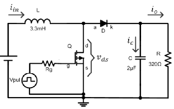
Figure 1. Primary variables of the boost converter
In this paper a measurement strategy, which is based on a compensation technique and a statistical design of experiments, has been proposed. The proposed strategy can compensate or minimize the most significant errors, produced by parasitic elements interacting with the switching devices, which are described in section 3. In order to validate the measurements and to obtain results with a good degree of accuracy, based on the obtained data, a statistical design of experiments is applied in section 4, which is an interesting approach to analyze the measurement problem due to experimental errors [12-14]. Afterwards, the design of experiments approach is proposed.
2. MEASUREMENT METHODOLOGY
The total power losses of a switching device, for any type of converter, are given by the switching and conduction losses. Instantaneous power is defined by (1). Then, in order to compute the total power losses the current and voltage instantaneous values are necessary.
 (1)
(1)
However, the addition of noises produced during the commutation process by parasitic elements, and other particular measurement problems, introduces errors in instantaneous voltage and current measurements; consequently, the instantaneous power computed by (1) is not correctly evaluated.
2.1 Definition of variables
The specific definition of variables and their location in the converter are neccessary in order to establish a general scheme of measurement. Once the variables are identified, the way to obtain the desired data is through the measured variables, which can be classified as primary or secondary variables.
2.1.1 Primary variables
Primary variables are signals that are measured directly from the converter by means of current and voltage probes. These signals have to be measured in adequate measurement points, taking into account that these are useful for analyzing circuit performance. Different primary variables and measurement points can be selected; however, such selection could require some circuit modifications due to the additional wiring needed to measure the current or other variables, which could increase the parasitic inductances or modify normal converter operation. For the Q switch case, the drain (id) current is deduced from equation (2). So, in order to keep original converter conditions, only three currents signals are considered as primary variables: input (iin), output (i0), and capacitor current (iC).
 (2)
(2)
Also, only one voltage signal is considered to be a primary variable: the drain-source voltage (vds). Since the source point of the Q switch is referred to the converter ground, vds is easily measured. Thus, Fig. 1 shows the primary variables.
2.1.2 Secondary variables
The secondary variables are not obtained by direct measurements; they are deduced from primary variables, based on some basic equations. Table 1 shows all the secondary variables considered in this work. In order to improve the secondary variables calculated, it is necessary to correct the errors and to compensate for the measurement affected by noise in the primary variables.
2.2 General Scheme
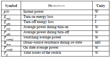
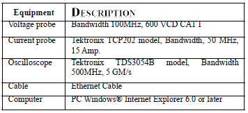
In order to obtain a reliable comparative study, good quality measurements have to be performed; it means that measurements have to contain minimal or no errors. Figure 2 shows the general measurement scheme. Firstly, the primary variables are measured by means of the current and voltage probes. Then, the acquired data are stored temporarily in the oscilloscope memory as time and amplitude vectors for the measured voltage and current signals. Then, by using the ethernet cable, all the stored vectors are transferred to the PC where data of the measured signals are processed in order to compensate for the errors and to compute the secondary variables. The different measurement noises and errors considered in this study are due to the circuit parasitic elements, and the current and voltage probes. Table 2 shows the measurement equipment used in this research.
Figure 2. General scheme of measurement
Table 2. Measurement equipment
3. MEASUREMENT ERRORS AND COMPENSATION TECHNIQUES
In this section we detail the different measurement errors and the compensation techniques used to correct the voltage and currents signals.
3.1 Asynchronous noise
Asynchronous noise is due to the addition of a greater number of individual fluctuating disturbances and, combined, can produce different waveforms for each individual repetition of the same measurement signal [15]. The technique used to eliminate or compensate for this kind of noise is based on the average of 128 acquisitions of the measured signal, see Figure 3. The signal-to-noise ratio is improved by N½, where N is the number of acquisitions [16]. The use of this compensation technique is limited by: a) the measured signal which has to be repetitive and b) the processing time, which is as big as the increase of N.
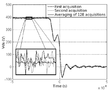
Figure 3. Asynchronous noise compensation
3.2 Synchronous noise
Synchronous noise disturbs the signal for every repetition in the same way [15], which means that the measured signal is composed of signal plus the synchronous noise. So the compensation technique to reduce the measurement error is applying the double measurement method [16], which consists of a) the first phase: the measurement of signal+noise (+unbalances), and b) the second phase: the measurement of noise (+unbalances). The measurement of noise consists of locating the probe in the same position without measuring the signal of interest. Figure 4 shows the compensation technique of ic obtained by applying this method. In order to compensate for the primary variables, the noise in the second phase has to be correctly measured. For measuring the noise of the voltage, the probe has to be referred to the ground. For measuring the noise of the current, the probe has to be located in the same place under currentless conditions.
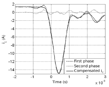
Figure 4. Synchronous noise compensation
3.3 Current and voltage probes delay time
The delay time between the voltage and current probes can introduce an important error for the instantaneous power losses calculation, using equation (1). The typical delay time for the probes listed in Table 2 is around 9.24 ns; this time becomes significant for the device commutation time. In order to avoid an important deviation, this time has to be compensated to correctly calculate the switching losses.
The delay time (Δt) can be characterized by applying a square signal to a purely resistive load, see Figure 5a. The delay time can be obtained from the measured voltage and current waveforms, as is shown in Figure 5b. The technique used to compensate for the delay time consists in introducing a phase shift (Δt), as is shown in (3).
 (3)
(3)
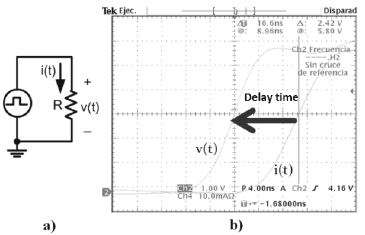
Figure 5. Probes delay time characterization: a) Test circuit, b) measured delay time
3.4 Inductances of device case
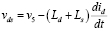
The parasitic inductances produce serious disturbances in the measured signals, caused by the high di/dt or dv/dt during device commutation. Figure 6 shows the parasitic elements in a boost converter, where the circuit layout parasitic resistances and inductances (LL1, LL2, L45, L43, L21, LR, LC1, LC2, L21, Lr1, Lr2, Lr3, RL, RC), and the parasitic inductances of the semiconductor device cases (Lg, Ld, Ls, La, Lk) can be identified. Parasitic elements of the layout circuit become important for estimating the secondary variables, whereas parasitic inductances of the device case are important to measure the MOSFET drain-source voltage (vds), which is strongly disturbed by the high did/dt during commutation, due to Ld and Ls inductances. The parasitic inductance values for CoolMOS IPA60R250CP are Ld=3nH and Ls=7nH. The voltage vds can be obtained by equation (4).
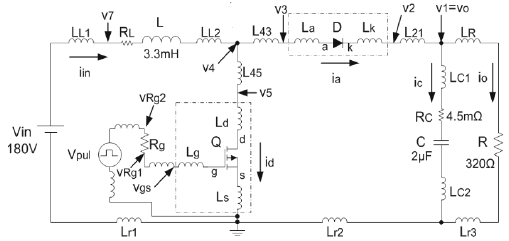
Figure 6. Boost converter with parasitic elements
 (4)
(4)
Additionally, a modification in the voltage probe has been implemented in order to minimize parasitic inductances. The ground wire was reduced, as Figure 7 shows.
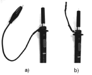
Figure 7. Voltage probe with ground wire a) 18.3 cm y b) 6.3 cm
3.5 On state voltage VDSON measurement
Figure 8 shows the error produced by an unbalanced voltage probe or saturation of the oscilloscope input channels. This is caused when a high voltage difference, around 400V applied to the probe, takes place in the commutation of the device, from blocking state (Vdsoff) to conduction state (Vdson). Consequentely, a strong saturation is produced in the oscilloscope input channels. The technique used to compensate for this problem is to limit the measured voltage seen by the probe. Figure 9 shows the circuit proposed for measuring low voltage during device conduction and the results of V6 are shown in Figure 10. The drain-source voltage Vdson is deduced from equation (5).
 (5)
(5)
Where vref is the reference voltage to correct the synchronous error and VDaux is the diode conduction, which has been previously characterized, see Figure 11.
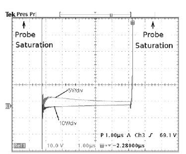
Figure 8. Saturation effect of the voltage probe for 10V/div and 5V/div scales
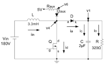
Figure 9. Proposed circuit to measure the Q switch conduction
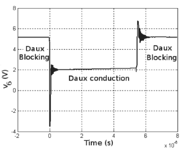
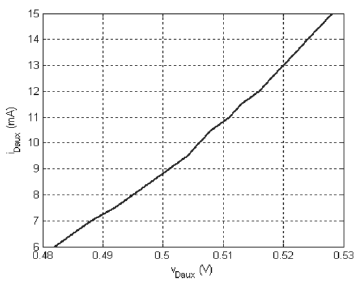
Figure 11. VDaux characterization
4. STATISTICAL DESIGN OF EXPERIMENTS
The design of experiments, based on statistical methodology, is an interesting approach to analyze problems involving data subject to experimental errors [14]. The aspects to be considered here are the following:
- Response variable. This is the dependent variable. Here, response variables can be selected from the set of secondary variables given in Table 1.
- Factors to change. These are the parameters of interest that influence the performance of the switch-diode couple. The factors which can be considered are: gate resistance (Rg); gate voltage (Vpul), commutation frequency (f ), and output power (P). In this paper, only the Rg factor is evaluated, but in the case of other factors being considered; it is important to note that only one factor has to be researched at a time.
- Treatment or levels. This is the set of values for the factor to evaluate. Here, the following set of values for Rg is considered: 1 Ω, 5.6 Ω, 10 Ω, and 15 Ω.
- Repetition or replica. This is the reproduction of a test (n) without changing the factor value. In this case n=3 repetitions have been suggested.
The statistical analysis of experiments has been developed for the case where the response variable is the swtching power losses (PconmQ). The analysis has three parts: 1) organization, register, and execution, 2) data collection and test results, and 3) statistical model validation.
1) Organization, register, and execution
Organization. Table 3 shows the numerical assignment of repetitions. After this, the repetitions are ordered in a random sequence corresponding to a progressive number, which is called the test sequence (sp); see Table 4.
Table 3. Numerical assignment for repetitions
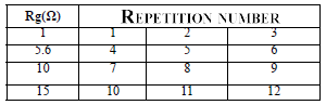
Table 4. Random sequence of repetitions
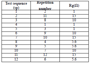
The random order of the test is intended to standardize the ambient conditions of the test.
Register and execution. The implementation of the experiment is developed for performing the measurement, as described previously. In this sense, twelve different values of Rg have been considered, as defined in Table 4. The registration implies storing measurement data, which includes parameter values, time vector, values of the measured variables for each test, the temperature of the heat sink, as well as the execution date.
2) Data recollection and test results
The purpose of the ANalysis of VAriance (ANOVA) is applied for analyzing the response variable under the same average [14]. Before performing the ANOVA, it is necessary to concentrate the data from the 12 tests as shown in Table 5. Then, based on MATLAB, the ANOVA is performed, which creates the table seen in Figure 12. From ANOVA, two important parameters to be considered are: 1) the statistic F = 20.96, which indicates that the average variability is 20.96 times bigger than that of the individual observations; 2) and the level of significance (p), shown as Prob>F, is 0.0004; which means a rejection that averages are equal, with an error probability of 0.04%. Figure 13 shows a graphic of PconmQ versus Rg, which is integrated by individual observations and their averages connected by a line.
Table 5. Execution of data by ANOVA
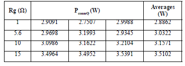
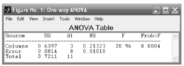
Figure 12. Results given by ANOVA table
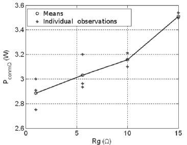
Figure 13. Graphic of PconmQ vs Rg
3) Statistical model validation
The analysis of variance is valid only when the observations of Table 5 match with the fixed-effect statistical model. This means that the residues must fulfill three basic requirements: an average equal to zero, normal distribution, and independence [14]. Firstly, the average of the residues is 3.7x10⁻¹⁷, which is almost zero. On the other hand, the normal distribution is verified when the cumulative probability in a graphic of normal probability is a straight line, as is shown in Figure 14. Figure 15 shows a graphic of residues (marked as circles) versus the adjusted values; it can be observed that there is no pattern, which indicates that the residues fulfill the requirement of independence.
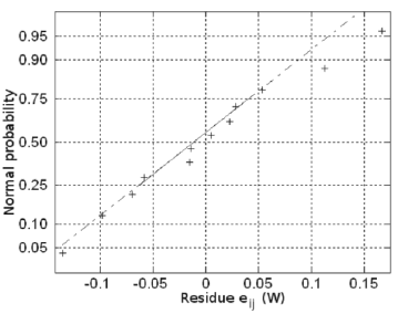
Figure 14. Normal probability of the residues
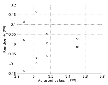
Figure 15. Graphic of the residues vs adjusted values
5. EXPERIMENTAL RESULTS
Figure 16 shows energy behavior during turn-on and turn-off commutation. The individual observations are marked as *, the averages for each level are marked as squares and joined by lines. Also, it can be observed that Rg has a high significant influence on EonQ, but very low influence on EoffQ. Figure 17 presents the turn-on and turn-off power losses; the behavior of these curves is similar to those in Figure 16, since it is the same information considering the switching frequency, which is 100 kHz. Figure 18 illustrates the switching, conduction and total losses as well as the significance values p for each curve. Finally, Figure 19 shows the behavior of Rdson when Rg is varying.
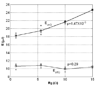
Figure 16. Turn-on and turn-off energy
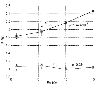
Figure 17. Turn-on and turn-off average power
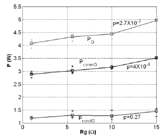
Figure 18. Commutation, conduction, and total average power losses
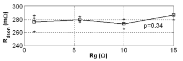
Figure 19. Rdson behavior under Rg variation
7. CONCLUSIONS
In this paper two very important topics have been considered in order to carry out the experiments: firstly, the experimental error compensations which improve the resulting measurements; secondly, the statistical design of experiments, which is a very useful tool to provide robustness for the results and conclusions obtained from the measurements data analysis.
The statistical approach offers confidence and certainty about the observed tendencies. If a repetition is realized for every value of the factor, it is possible to reduce the false tendencies. Additionaly, the repetitions and the random sequence help to accomplish the real value of the measured signals. Also, the significance value p helps to interpret the tendency of the curves. If p is very small, as in the case of EonQ, PonQ, PconmQ, and PQ, it clearly indicates that there is an influence of Rg. On the other hand, if p is higher, as in EoffQ, PoffQ, PcondQ, and Rdson, it is not possible to establish the influence of Rg with so much confidence; it is even possible to say that Rg has no influence.
Finally, the combination of the compensation of errors and the statistical design of experiments is a very powerful tool for obtaining information and highly reliable results.
REFERENCES
[1] ERICKSON R. W., MAKSIMOVIC D. Fundamentals of Power Electronics, Second Edition, Springer Science+Bussines Media, Inc. New York, USA, 2001. [ Links ]
[2] D. D. LU, J. C. P. LIU, F. N. K. POON, B. M. H. PONG, "A single phase voltage regulator module (VRM) with stepping inductance for fast transient response", IEEE Transactions on Power Electronics, Vol.22, no 2, March 2007, pp. 417-4242. [ Links ]
[3] J. HAN, A. JOUANNE, G. C. TEMES, "A new approach to reducing output ripple in switched-capacitor-based step-down dc-dc converters", IEEE Transactions on Power Electronics, vol. 21, no. 6, November 2006, pp 1548-1555. [ Links ]
[4] JOVANOVIC M., JANG Y. "State-of-the-art, Single-Phase, Active-Power-Factor-Correction Techniques for High-Power Applications – An Overview". IEEE Transactions on Industrial Electronics, Vol 52, no.3, June 2005. [ Links ]
[5] FERNANDO VILLADA DUQUE, RICARDO A. VELÁSQUEZ V, DIEGO R. CADAVID C, "Design And Construction Of A Digital Prototype To Diagnose Faults In Induction Motors", Revista DYNA, November 2007, No 153, pp 215-222. [ Links ]
[6] R. M. ABOU-ALFOTOUH, A. V. RADUN, H. R. CHANG, C. WINTERHALTER, "A 1-MHz hard switched silicon carbide DC-DC converter", IEEE Transactions on Power Electronics, Vol. 21, no. 4, July 2006, pp. 880-889. [ Links ]
[7] S. MUSUMECI, A. RACITI, F. FRISINA, M. MELITO, M. G. SAGGIO, "Performance analysis of merged p-i-n-Schottky diodes with doping compensation of the drift region", IEEE Transactions on Industry Applications, Vol. 43, no. 3, May/June 2007, pp. 636-647. [ Links ]
[8] YAO K., LEE F. C, "A Novel Resonant Gate Drive for High Frequency Synchronous Buck Converters". IEEE Trans. on Power Electronics, Vol. 17, no. 2, March 2002, pp 180-186. [ Links ]
[9] SPIAZZI G., BUSO S., CITRON M., CORRADIN M. AND PIEROBON R, "Performance Evaluation of Schottky SiC Power Diode in a Boost PFC Application". IEEE Trans. on Power Electronics, Vol. 18, no 6, November 2003, pp 1249-1253. [ Links ]
[10] LORENZ L, DEBOY G, ZVEREV I, "Matched pair of CoolMOS transistors with SiC-Schottky diode–advantages in application", IEEE Trans. on Industry Applications, Vol. 40, no. 5, September/October 2004, pp. 1265-1272. [ Links ]
[11] CHIMENTO F., MUSUMECI S., RACITI A., MELITO M., SORRENTINO G, "Super-Junction MOSFET and SiC Diode Application for the Efficiency Improvement in a Boost PFC Converter", 32nd IEEE Annual Conference on Industrial Electronics, IECON 2006, November 2006, pp. 2067-2072. [ Links ]
[12] JUAN CARLOS SALAZAR, ARMANDO BAENA ZAPATA, "Analysis and design of experiments applied to simulation studies". Revista DYNA, 2009, No 159, pp 249-257. [ Links ]
[13] ALEXANDER CORRE, ATALINA M. BURGOS, "Design and implementation of a statistical methodology for rehearsals of finished product in cements el Cairo S.A", Revista DYNA, 2007, No 151, pp 195-207. [ Links ]
[14] MONTGOMERY D.C., Diseño y Análisis de Experimentos. México, Iberoamerica Editorial Group, 1991. [ Links ]
[15] GUTIÉRREZ C. Introducción a la metodología experimental. México. Second edition, LIMUSA, 2006. [ Links ]
[16] CAUFFET G. Optimisation dune chaine des measures electriques pour lelectronique de puissance. France, PhD dissertation, INP of Grenoble, 1992. [ Links ]

