


Services on Demand
Journal
Article
 English (pdf)
 Article in xml format
 Article references
 Send this article by e-mail
Indicators
-
 Cited by SciELO
 -
 Access statistics
Related links
-
 Cited by Google
 -
 Similars in
SciELO
Similars in
SciELO -
 Similars in Google
Share

 Permalink
DYNA
Print version ISSN 0012-7353On-line version ISSN 2346-2183
Dyna rev.fac.nac.minas vol.79 no.171 Medellín Jan./Feb. 2012
DESIGN OF ASYMMETRICAL BOOST CONVERTERS BASED ON PHOTOVOLTAIC SYSTEMS REQUIREMENTS
DISEÑO DE CONVERTIDORES ELEVADORES ASIMÉTRICOS PARA APLICACIONES FOTOVOLTAICAS
ELIANA ISABEL ARANGO ZULUAGA
Ph.D., Profesor Facultad de Minas, Universidad Nacional de Colombia, Sede Medellín, eiarangoz@unal.edu.co
CARLOS ANDRÉS RAMOS-PAJA
Ph.D., Profesor Facultad de Minas, Universidad Nacional de Colombia, Sede Medellín, caramosp@unal.edu.co
ANDRÉS JULIÁN SAAVEDRA-MONTES
Ph.D., Profesor Facultad de Minas, Universidad Nacional de Colombia, Sede Medellín, ajsaaved@unal.edu.co
Received for review June 10th, 2011, accepted November 28th, 2011, final version December, 5th, 2011
ABSTRACT: An asymmetrical interleaved dual boost DC/DC switching converter is proposed to improve photovoltaic systems. Such a new step-up power converter provides a low input current ripple injected into the photovoltaic generator, and at the same time provides a low voltage ripple to the load. The developed converter is based on traditional interleaved boost converters interacting with voltage multiplier cells where the circuit symmetry has been broken, obtaining an inherent discontinuous conduction-operating mode that provides a high voltage conversion ratio in comparison to traditional solutions. Such low-ripple and high boosting conditions make this converter an ideal candidate for photovoltaic systems design, in particular for grid-connected applications. The converter circuitry is analyzed, and a design procedure is proposed in terms of typical photovoltaic systems requirements, providing simple but useful equations. Finally, the converter design is illustrated by means of a realistic design example and validated by using an experimental prototype.
KEYWORDS: photovoltaic systems, DC/DC switching converters, asymmetrical interleaved, discontinuous conduction mode
RESUMEN: Este artículo presenta un convertidor conmutado DC/DC elevador, entrelazado y asimétrico, propuesto para interactuar con sistemas fotovoltaicos. Este nuevo convertidor provee condiciones de bajo-rizado de corriente al generador fotovoltaico y de bajo-rizado de voltaje a la carga. Así mismo, el convertidor está basado en estructuras entrelazadas típicas interactuando con celdas multiplicadoras de voltaje, donde la simetría del circuito se rompe para obtener un convertidor que opera inherentemente en modo de conducción discontinuo que provee una razón de elevación de tensión superior a las soluciones tradicionales. Las características de bajo rizado y alta elevación hacen de este convertidor un candidato ideal para interactuar con sistemas fotovoltaicos, y en particular con sistemas conectados a la red eléctrica. El convertidor es analizado circuitalmente, y se propone un procedimiento de diseño basado en requerimientos típicos de los sistemas fotovoltaicos, presentando ecuaciones de diseño simples pero útiles. Finalmente, el diseño del convertidor se ilustra a través de un ejemplo de diseño realista, y se valida usando un prototipo experimental.
PALABRAS CLAVE: sistemas fotovoltaicos, conversores DC/DC conmutados, entrelazado asimétrico, modo de conducción discontinuo
1. INTRODUCTION
Photovoltaic power systems are efficient alternatives to provide electrical energy providing redundancy for critical applications, in situ energy generation [1], and the reduction of traditional energy generation that impacts the environment. Similarly, photovoltaic generators have been intensively used in residential applications [2-4], and autonomous and portable applications [5].
Photovoltaic systems require a power electronics interface to define their operating point at optimal conditions for any load or grid-connection. This aspect has been addressed by single-stage inverters [6], or by adopting double-stage structures based on DC/DC and DC/AC converters [7]. The double-stage approach is widely accepted due to its application in distributed generation system based on multiple generators [2], as well as in stand-alone DC applications, where a single DC/DC converter is required [4].
The PV applications commonly adopt boosting converters for grid-connected applications due to the requirement of increasing the voltage to the grid-connected inverter operating conditions. The most commonly used DC/DC converter in the first stage of such systems is the classical boost converter [2,7], which provides an acceptable voltage conversion ratio, and also requests a continuous current from the photovoltaic (PV) panel. Other characteristics required in PV applications are a low current ripple injected to the PV and high conversion efficiency. The current ripple magnitude is an important factor in the selection of power converters for PV applications because high current ripples produce an oscillation around the maximum power point (MPP) [8,9] that reduces the energy extracted from the PV generator.
The boost converter is a good candidate for interfacing PV systems among other converters [2,7]. But in such a boost converter, the current ripples injected to the PV generators depend on the inductor size, switching frequency, input capacitor, and high frequency power source impedance; therefore, in order to reduce the current ripple, it is necessary to increase the converter inductance or input capacitance, modifying the dynamics of the system. This can be addressed by using an additional filter between the PV generator and the power converter, also increasing power losses, size, weight, cost, and the order of the system. Another possibility for reducing the converter's input current ripple is given by the interleaving structures [10], which considers the connection of DC/DC converters in parallel to share the power flow between two or more branches. This implies a reduction in the size, weight, and volume of the inductors and capacitors [11]. In addition, a proper control of the parallel converters increases the ripple frequency and reduces the ripple waveforms at the input and output of the power conversion system [12], which leads to a significant reduction of the current and voltage ripples. The interleaving solution has been successfully adopted in photovoltaic applications [8], but traditional interleaving structures require current control loops in each phase to ensure proper current sharing among the parallelized converters, since differences in the phase impedances causes imbalances in the phase currents.
To achieve a high voltage conversion ratio, it is possible to use voltage multiplier cells to increase the traditional DC/DC converters voltage conversion ratio [13]. This solution impacts the behavior of the original power converter and the resulting circuit can be operated in continuous (CCM) or discontinuous (DCM) conduction mode. In PV systems, power converters can be operated in both CCM [2,9] and DCM [6], depending on the power converter design.
This paper proposes an asymmetrical interleaved dual boost converter (AIDB) topology and design procedure for photovoltaic power systems. The AIDB has been developed from the traditional interleaved boost converter interacting with voltage multiplier cells to provide higher conversion ratio compared with the traditional structure, but preserving the characteristic of small input current and output voltage ripples. In addition, the AIDB does not require internal current control loops to ensure current sharing among the parallelized converters [12], which reduces the complexity of the overall control system.
Moreover, the AIDB exhibits an inherent DCM operation, which in traditional and interleaved DC/DC converters [14,15], implies a dependency of the voltage conversion ratio from the circuit parameters and load impedance, making it difficult to design for non-constant load conditions. In contrast, the AIDB voltage conversion ratio does not depend on the circuit or load parameters.
The remaining part of the paper is organized as follows: in Section 2 the AIDB converter circuital analysis is performed and a design process for PV applications is proposed. Then, Section 3 illustrates the AIDB topology and design by means of an application example experimentally validated. Finally, the conclusions are given in Section 4.
2. ASYMMETRICAL INTERLEAVED DUAL BOOST ANALYSIS AND DESIGN
The interleaving technique consists in the parallel interconnection of a determined number of identical converters, in which control signals are strategically phase shifted in each switching period. This arrangement reduces the net ripple amplitude through harmonic cancellation and raises the effective ripple frequency of the overall converter without increasing switching losses or device stresses, and divides the input power between the branches. An interleaved system reduces the ripple filtering requirements, the conduction losses, and prototype size without sacrificing conversion efficiency [10].
In the interleaved interconnection of two switching converters, the ripples can be significantly reduced by using two optimal configurations: when one switch is ON at the same time that the other one is OFF. In these optimal configurations, the inductor current of one converter is increasing while the other inductor current is decreasing, therefore the inductor current waveforms of the two converters have slopes with opposite signs, while the slope of the total interleaved input current is reduced, as well as its ripple. Consequently, if the aim is to obtain low input and output ripples, the interleaved circuit has to be controlled to turn on the switches in a complementary way. This complementary interleaving offers more simplicity in the control design than other kinds of interleaving, because one activation signal is the opposite of the other activation signal [11].
The asymmetrical interleaved dual boost or AIDB, was obtained from the traditional interleaved dual boost (IDB) converter [8]—whose circuital scheme is given in Fig.1—by connecting a voltage multiplier cell [13] at its output port. Then, the order of the output filter was increased to reduce the output voltage ripple, done by introducing inductive filters at the branch outputs. Such a structure exhibits a similar behavior to the IDB [11], where the CCM operating condition is constrained to duty cycles near to 0.5; therefore, it is not possible to regulate it. To avoid this limitation, the symmetry of the structure is broken, obtaining the asymmetrical circuit depicted in Fig. 2, where, in addition, the power source is now a PV panel.
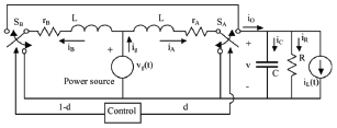
Figure 1. IDB circuital scheme.
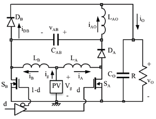
Figure 2. AIDB circuital scheme
The AIDB is basically a parallel interconnection between a boost converter with an output filter (branch A) and a traditional boost converter (branch B) in which the first capacitor of the A-branch output filter is connected to the intermediate node of the boost of the B-branch. This method follows the concept of switching capacitor-based voltage multiplier cells. The MOSFETs SA and SB are activated in a complementary way to obtain the desired input current ripple reduction.
2.1 Circuit analysis and topologies
In the following, lowercase letters refer to dynamic variables and uppercase letters refer to steady-state variables.
The sequence of operation intervals, which have the respective duration of d1T, d2T, and d3T, can be defined using Fig. 3 which shows the DCM currents in the AIDB circuit, without loss of generality, for a duty cycle of 50%. The definition of the operation intervals is the following:
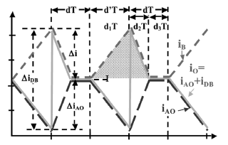
Figure 3. AIDB operation intervals
Figure 4 shows the topologies of the converter in each operation interval. The topologies were identified using both the simulation waveforms and the usual procedure of assuming all the possible positions in the switches. The states of the switches in the four topologies are defined as:
- Topology 1: SB and DA ON; SA and DB OFF. Interval 1: d' = d1
- Topology 2: SA and DB ON; SB and DA OFF. Interval 2: d2
- Topology 3: SA ON; SB, DA and DB OFF, where DB is in DCM. Interval 3: d3
- Topology 4: SB ON; SA, DA and DB OFF, where DA is in DCM
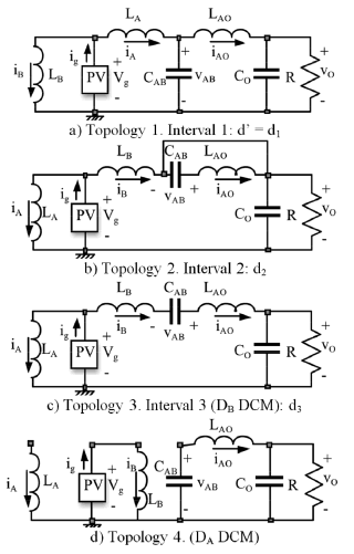
Depending on the duty cycle, two operation sequences may occur: For duty cycles greater than 0.382, the converter structure follows topologies 1, 2, and 3; while for duty cycles lower than 0.382, the converter structure changes into topologies 1, 4, and 2. In the first sequence, which is the one for the desired operation, the transition from topology 1 to topology 2 occurs by the change of the MOSFET states. The transition from topology 2 to topology 3 takes place when iB and iAO are equal, therefore the diode DB current becomes zero. Finally, the transition from topology 3 to topology 1 is driven by the change of the MOSFET states. Similarly, in the second sequence, which is a not the desired one, the transition from topology 1 to topology 4 occurs when iA current becomes zero. The transitions from topology 4 to topology 2 and from topology 2 to topology 1 are driven by the change of the MOSFET states.
The operation sequence 1-2-3 provides low input current and output voltage ripples, which are required for photovoltaic systems. The low ripple conditions are due to the continuous waveform of the LA inductor current, therefore it produces a low harmonic content. On the contrary, sequence 1-4-2 forces both LA and LB discontinuous inductor currents producing a high harmonic content.
From the AIDB topologies depicted in Fig. 4, a permanent loop is found: voltage source Vg, inductors LB and LAO, and capacitors CAB and CO. Considering the converter in steady-state [14], Eq. (3) can be obtained from the permanent loop, where VAB represents the CAB voltage, Vg the input voltage, and VO the output voltage.
Similarly, from the amplitude of the LA current ripple on the first and second or third topologies, the expressions for steady-state VAB and output voltage VO are given by (4) and (5), respectively.
where the voltage conversion ratio for the AIDB converter is given by (6), which is higher than the one provided by the traditional boost converter (7) [14] for the same duty cycle.
Analyzing the permanent loop in topology 3, it is found that the voltages on LB and LAO have an equal magnitude but the opposite sign (8), while LB and LAO are series, therefore their currents are equal (9). Then, deriving (9), the relation given by (10) is found.
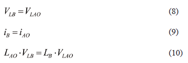
The solution for the equation system (8-10) is VLB=VLAO=0, which implies that iB and iAO are equal and constant in the interval D3T.
From the ripple amplitude of the LB current in the first and second topologies, taking into account the output voltage magnitude (5) and intervals duration relations (1-2), D2, and D3 are given by:
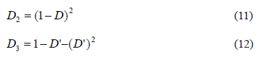
It is noted that the AIDB intervals duration and voltage conversion ratio do not depend on the converters or load parameters despite their DCM operation. This is an improvement over classical converters such as boost, buck, or buck-boost.
From (12) it is found that D = 0.382 defines an operation limit for the converter, because 0 < D < 0.382 imply D3 < 0, therefore the AIDB is not operating in the desired sequence 1-2-3.
The average current in CAB in the first, second, and third topologies is given by IA-IAO, -IAO, and -IAO = -IB, respectively, where capitol letters corresponds to the steady state currents of LA, LAO, and LB. From the charge balance on CAB and taking into account that D2 + D3 = D as given in (2), the relation between IA and IAO is given by IA = IAO/D'. Similarly, from the steady state charge balance on the output capacitor CO, taking into account that in topologies 2 and 3 the average output current is supplied exclusively by LB, from the series connection of LB and LAO in the third topology, and from the D2 and D3 length (11-12), the relation between IAO and IB is IAO = IB. From the previous analyses and the AIDB voltage conversion ratio, the AIDB steady state inductors currents are:
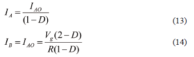
Equation (14) shows that the current sharing among LA and LAO is naturally defined by the AIDB structure without any additional control loops, and Eq. (13) gives information about the inductor current ratings, where it is noted that LA inductor must be heavier and bulkier than LAO and LB.
2.2 Design procedure and equations
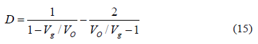
The proposed AIDB design process is intended to fulfill typical requirements in photovoltaic systems. The aspect imposed is the voltage conversion ratio since PV generators define the AIDB input voltage, while the load specifications define the converter output voltage; i.e., grid connected inverter. The steady state duty cycle for given input and output voltages is:
The input current ripple amplitude is another important condition to be designed. In this way, the amplitude of the AIDB input current ripple corresponds to the magnitude difference between LA and LB current ripples, which in topologies 1, 2, and 3, are given by (16), (17), and (18), respectively.
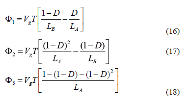
Taking into account that the converter steady-state condition, F1 + F2 + F3 = 0, which implies that the magnitude of the larger ripple section must be equal to the sum of the magnitudes of the other ones. Adopting the design condition LA = LB = L, it is noted that F1 < F2 for 0.382 < D < 1, F1 < F3 for 0.439 < D < 1, and F2 < F3 for 0.5 < D < 1. Such relations allow for one to define a design equation for LA and LB as
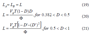
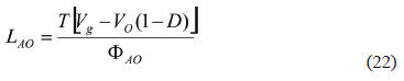
where F represents the desired input current ripple magnitude. Similarly, LAO inductor can be designed in agreement with the desired inductor current ripple FAO as
In addition, LAO = LB condition provides a triangular waveform of the CAB voltage, which is a convenient condition for classical control-oriented modeling approaches [14].
Moreover, the input current ripple magnitude F will impact the power produced by the PV module since it generates an undesired oscillation around the desired operating point. To analyze this effect, the small signal equivalent circuit of the PV module-AIDB converter is depicted in Fig. 5, where the AIDB input current, in steady-state, can be modeled by ig(t) = F(t) + Ig(t). F(t) represents the small-signal oscillation and Ig(t) the steady-state current. In the model, Rmpp = Vmpp/Impp represents the small-signal behavior of the PV module [16] named PV module differential resistance, while Vmpp and Impp are the PV voltage and current at the maximum power point (MPP). Since a PV generator exhibits an optimal operating condition or MPP, a control algorithm to track such a condition, named the maximum power point tracking (MPPT) controller, is necessary.
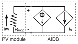
Figure 5. PV-AIDB connection: small signal model
Taking into account that a properly designed MPPT controller provides an MPPT efficiency higher than 99% [16], the oscillation on the power due to the AIDB input current ripple must be lower than 0.1% to avoid sensible additional losses; therefore, the current ripple magnitude that generates such a maximum desired power oscillation FP can be approximated by
where Pmpp represents the PV power and the MPP.
The CAB capacitor design must be performed in order to guarantee a maximum allowed capacitor voltage ripple FAB to avoid damages in transient conditions. Equation (25) gives the CAB value that ensures a maximum FAB for a desired load impedance R, duty cycle D, and CAB steady state voltage VAB.
The design of the output capacitor CO is performed to fulfill a given output voltage ripple requirement FO. From the second order filter analysis given in [14], Eq. (26) provides the CO value to for a given duty cycle and LAO conditions.
3. APPLICATION EXAMPLE
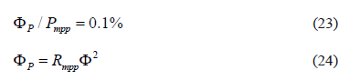
This AIDB design example considers a grid connected PV application that requires a step-up condition to meet the inverter stage input voltage level [6]. In addition, a PV panel Sharp NU-U235F1 is considered, which consists of three cell-strings in series, each one of them equipped with a by-pass diode [16]. Consequently, the NU-U235F1 is composed by three PV modules, each one of them exhibiting Pmpp = 78 W, Vmpp = 10 V, Impp = 7.84 A, open circuit voltage Voc = 12.33 V, and short-circuit current Isc = 8.60 A, all of those parameters are measured under standard test conditions (STC). The current-voltage (I-V) and power-voltage (P-V) characteristic curves for a single PV module of such a commercial PV panel are depicted in Fig. 6, where 1000 W/m2, 800 W/m2, and 600 W/m2 irradiance conditions are illustrated.
Figure 6. I-V and P-V curves for the Sharp NU-U235F1: single module
For a typical 500 W and 120 VAC grid-connected full-bridge inverter, the PV system requires two NU-U235F1 PV panels that correspond to 95% of the maximum inverter power. The full-bridge inverter requires approximately 170 VDC to meet the desired grid voltage, and to provide an additional 5% of safe margin to compensate for parasitic losses, this example considers the input voltage of the inverter equal to 180 V. Such a condition defines the AIDB input and output voltages Vg = 10 V and VO = 30 V, respectively; therefore, the duty cycle in the MPPT conditions is D = 0.5 as given in (15). It is noted that a 500 W PV system with two NU-U235F1 PV panels requires 6 AIDB converters, one for each PV module, all of them identical. Therefore, this example presents the design and experimental validation of a single converter.
For the considered NU-U235F1 PV modules, Rmpp = 1.276 W, FP = 78 mW, and F = 247.3 mA. In addition, the switching frequency was selected as fsw = 50 kHz; therefore, the switching period T = 20 ms. From Eqs. (19-21), the input inductors are calculated to be equal to 202.18 mH, where near commercial inductors LA = LB = 200 mH were found. Similarly, to obtain a CAB triangular voltage waveform, LAO = LB = 200 mH was adopted.
In the same way, CAB and CO have been designed to achieve small voltage ripples using Eqs. (25) and (26), respectively. In this example, FAB = 3% and FO = 0.4% have been defined, but it is noted that any other requirements can be imposed. From such conditions, CAB = 50 mF and CO = 20.83 mF, where the capacitances achievable with commercially available capacitors were CAB = 50 mF with five 10 mF capacitors, and CO = 23.5 mF with five 4.7 mF capacitors.
The AIDB experimental prototype has been implemented as depicted in Fig. 7(a), where the three inductors and two capacitors banks are observed. In such an experimental prototype, the measured series resistances in LA, LB, and LAO were RLA = 34 mW and RLB = RLAO = 66 mW, respectively. Similarly, the series resistances in CAB and CO were RCAB = RCO = 81 mW, the MOSFETs and DIODEs used were IRFP054 and MBR1045, respectively, and a complementary output IR4428 driver was used to manage both MOSFETs. Figure 7(b) shows the laboratory set-up used to perform the experimental measurements, which validate the AIDB design procedure and equations.
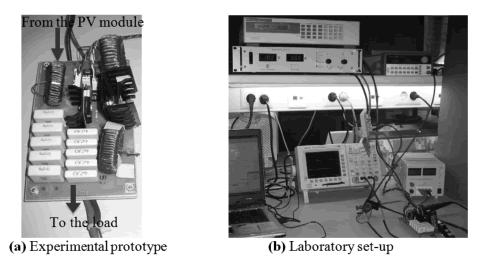
Figure 7. AIDB experimental test bench
The operating conditions of the AIDB experimental prototype have been defined in agreement with the design example requirements: 10 V input voltage and 7.68 input current, duty cycle equal to 50%, and a 30 V load voltage. Figure 8(a) shows the experimental LB and LAO currents, where the AIDB inherent DCM operating condition is exhibited, validating the Fig. 3 analyses since both figures are in agreement, and illustrating the three operating intervals d1, d2, and d3, which additionally puts the operation in the sequence 1-2-3 in evidence.
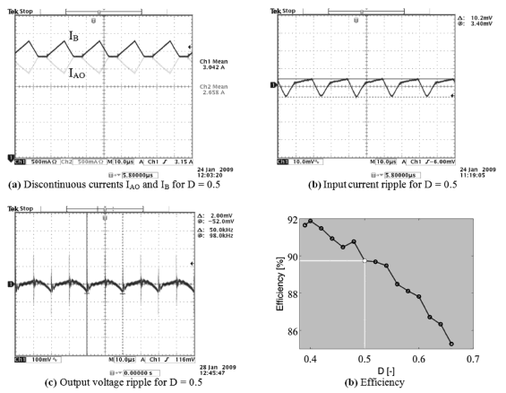
Figure 8. AIDB experimental measurements
Figure 8(b) depicts the experimental AIDB input current waveform, where the small input current ripple condition imposed in the design process is achieved. The current ripple has been measured by using a current-to-voltage sensor with a gain equal to 25 mV/mA, reporting F = 255 mA that corresponds to an error of 3% over the designed value. Similarly, Fig. 8(c) presents the experimental output voltage ripple, whose amplitude is in agreement with the design example calculation given by Eq. (26), exhibiting an error of 6% over the theoretical prediction. Moreover, Fig. 8(d) presents the efficiency of the experimental prototype for duty cycle conditions within 0.382 < D < 0.660, which at the particular design operating point (D = 0.5) is equal to 89.74%. It is noted that the experimental duty cycle range must be limited to D > 0.382 in order to guarantee the AIDB operation in the low-ripple sequence 1-2-3.
Finally, the experimental results exhibit a satisfactory agreement with the design calculations, validating the proposed design process.
4. CONCLUSIONS
An asymmetrical interleaved dual boost converter designed to interact with photovoltaic systems has been proposed, analyzed, and experimentally validated. The converter was developed by breaking the symmetry of traditional interleaved boost converters with voltage multiplier cells.
The proposed AIDB converter provides reduced input current and output voltage ripples for duty cycles higher than 0.382, while in other conditions the converter operates in an undesired and non-optimal topologies sequence. Moreover, the AIDB exhibits an inherent DCM condition that causes a natural current sharing among the parallelized branches without any additional current controller, while its voltage conversion ratio does not depend on converter or load parameters like in conventional DCM converters, which will simplify a regulation strategy design for the AIDB converter. Moreover, the AIDB small input current and output voltage ripple conditions avoid power losses due to oscillations around the PV panel MPP, and at the same time provide a high quality power supply to the load by avoiding undesired current and voltage harmonics.
The AIDB design process has also been proposed, which is based on typical photovoltaic systems requirements. Such a design procedure has been illustrated and experimentally validated by means of laboratory tests on a real AIDB prototype. The measurements show a satisfactory agreement with the theoretical predictions.
Finally, the operation of the AIDB converter can be improved by adopting non-linear control strategies, like the one proposed in [17], to reject environmental or load perturbations.
ACKNOWLEDGEMENTS
This work was supported by the the Universidad Nacional de Colombia, and by Colciencias under scholarship #095-2005.
REFERENCES
[1] Ouyang, W., Cheng, H., Zhang, X., and Yao, L., Distribution network planning method considering distributed generation for peak cutting, Energy Conversion and Management, vol. 51, pp. 2394-2401, 2010. [ Links ]
[2] Ahmed, N. A., Miyatake, M., and Al-othman, A. K., Power fluctuations suppression of stand-alone hybrid generation combining solar photovoltaic/wind turbine and fuel cell systems, Energy Conversion and Management, vol. 49, pp. 2711-2719, 2008. [ Links ]
[3] Al-salaymeh, A., Al-hamamre, Z., Sharaf, F., and Abdelkader, M. R., Technical and economical assessment of the utilization of photovoltaic systems in residential buildings: The case of Jordan, Energy Conversion and Management, vol. 51, pp. 1719-1726, 2010. [ Links ]
[4] Benghanem, M., Low cost management for photovoltaic systems in isolated site with new IV characterization model proposed, Energy Conversion and Management, vol. 50, pp. 748-755, 2009. [ Links ]
[5] Soler-bientz, R., Ricalde-cab, L. O., and Solis-Rodriguez, L. E., Developing a mobile stand alone photovoltaic generator, Energy Conversion and Management, vol. 47, pp. 2948-2960, 2006. [ Links ]
[6] Jain, S. and Agarwal, V., New current control based MPPT technique for single stage grid connected PV systems, Energy Conversion and Management, vol. 48, pp. 625-644, 2007. [ Links ]
[7] Ilango, G. S. and Rajasekar, N., An improved energy saving v/f control technique for solar powered single-phase induction motor, Energy Conversion and Management, vol. 50, pp. 2913-2918, 2009. [ Links ]
[8] Veerachary, M. and Uezato, T. S. A. K., Maximum power point tracking control of IDB converter supplied PV system, IEE Proceedings - Electric Power Applications, vol. 148, pp. 494-502, 2001. [ Links ]
[9] Aranda, E. D., Galan, J. A. G., Cardona, M. S. D., and Marquez, J. M. A., Measuring the I-V curve of PV generators, IEEE Industrial Electronics Magazine, vol. 3, pp. 4-14, 2009. [ Links ]
[10] Giral, R., Martinez-Salamero, L., and Singer, S., Interleaved converters operation based on CMC, IEEE Transactions on Power Electronics, vol. 14, pp. 643-652, 1999. [ Links ]
[11] Giral, R., Martinez-Salamero, L., Leyva, R., and Maixe, J., Sliding-mode control of interleaved boost converters, IEEE Transactions on Circuits and Systems I: Fundamental Theory and Applications, vol. 47, pp. 1330-1339, 2000. [ Links ]
[12] Thounthong, P. and Davat, B., Study of a multiphase interleaved step-up converter for fuel cell high power applications, Energy Conversion and Management, vol. 51, pp. 826-832, 2010. [ Links ]
[13] Prudente, M., Pfitscher, L. L., Emmendoerfer, G., Romaneli, E. F., and Gules, R., Voltage Multiplier Cells Applied to Non-Isolated DC-DC Converters, IEEE Transactions on Power Electronics, vol. 23, pp. 871-887, 2008. [ Links ]
[14] Erickson, R. W. and Maksimovic, D., Fundamentals of power electronics, Springer, 2nd, 2001. [ Links ]
[15] Ray, B., Kosai, H., Mcneal, S., Jordan, B., and Scofield, J., Performance analysis of a multi-mode interleaved boost converter, IEEE Energy Conversion Congress and Exposition - ECCE, vol. 1, pp. 2176-2183, 2009. [ Links ]
[16] Femia, N., Petrone, G., Spagnuolo, G., and Vitelli, M., A Technique for Improving P&O MPPT Performances of Double-Stage Grid-Connected Photovoltaic Systems, IEEE Transactions on Industrial Electronics, vol. 56, pp. 4473-4482, 2009. [ Links ]
[17] Angulo, F., Olivar, G., and Osorio, G. A., Generalization of ZAD strategy: An application to a dc-dc buck converter, DYNA, vol. 166, pp. 98-107, 2011. [ Links ]

