


Serviços Personalizados
Journal
Artigo
 Inglês (pdf)
 Artigo em XML
 Referências do artigo
 Enviar este artigo por email
Indicadores
-
 Citado por SciELO
 -
 Acessos
Links relacionados
-
 Citado por Google
 -
 Similares em
SciELO
Similares em
SciELO -
 Similares em Google
Compartilhar

 Permalink
DYNA
versão impressa ISSN 0012-7353
Dyna rev.fac.nac.minas vol.79 no.174 Medellín jul./ago. 2012
LOCAL ANODIC OXIDATION ON SILICON (100) SUBSTRATES USING ATOMIC FORCE MICROSCOPY
OXIDACION ANODICA LOCALIZADA EN SUBTRATOS DE SILICIO (100) USANDO MICROSCOPÍA DE FUERZA ATÓMICA
ALBA GRACIELA ÁVILA BERNAL
PhD. Profesora Asociada, Universidad de los Andes, a-avila@uniandes.edu.co
RUY SEBASTIÁN BONILLA
MPhil., Profesor Instructor, Universidad de los Andes, bonilla10@gmail.com
Received for review November 23th, 2011, accepted February 28th, 2012, final version March, 21th, 2012
ABSTRACT: A characterization of local anodic oxidation using scanning probe microscopy is performed on a (100) silicon substrate. The formation of patterns varies as a function of voltage, humidity, and scanning speed. A set of experiments is presented to analyze the voltage and scanning speed dependence under stable environmental conditions (50.5% relative humidity, 22 °C, and 767 mmHg). A finer control of the dimensions of the local oxidation patterns is attained at low voltages and low scanning speeds. Oxide ridges are observed at high voltages independently of the writing speed. Their presence sets up an upper limit for the oxide pattern formation.
KEYWORDS: LAO, AFM, Nano-patterns
RESUMEN: Se reporta la caracterización de la oxidación anódica local utilizando microscopía de barrido de la sonda sobre un substrato (100) de silicio. La formación de patrones varía como una función del voltaje aplicado, la humedad y velocidad de barrido. Se describe una serie de experimentos para analizar el efecto del voltaje y la dependencia de la velocidad de barrido bajo condiciones ambientales estables (50,5% de humedad relativa, 22 °C, y 767mmHg). Un mayor control de las dimensiones de lo patrones de oxido se logra a bajos voltajes y velocidades de barrido. Fracciones discretas de óxido se observan a altos voltajes independientes de la velocidad de barrido. La presencia de estos fragmentos fija un límite superior para la formación de patrones de óxido.
PALABRAS CLAVE: LAO, AFM, Nano-patrones
1. INTRODUCTION
Since the birth of scanning probe microscopy (SPM) with the invention of the scanning tunneling microscope back in 1982 [1], this instrument has provided scientists with a very powerful and versatile technique to visualize, characterize, and manipulate atoms.
A biased conductive tip in the atomic force microscope AFM, acts as a conductive electrode to provide stimuli and monitor surface changes. This characteristic extends the AFM's application to local anodic oxidation (LAO). Local anodic oxidation is an SPM-enhanced technique that allows for the fabrication of a variety of oxide compounds with different geometries on metallic or semiconductor substrates, with a feature size ranging from 1 to 100 nanometers. In previous studies, LAO has been demonstrated on sputtered titanium films of 10 nm [1] and 50 nm [2], as well as in silicon substrates n-type [3,4] and p-type [5]. Moreover, works have been reported on different applications of these techniques (i.e., for mask-making from SiNWs with different geometries [6], quantum dots [7], and single electron transistors [8]).
This paper is written with the intention of setting the experimental parameters for the local application of this technique. It focuses on the study of how voltage and writing speed impact the height and width of oxide nano-patterns, establishing the ranges and rates for controlled pattern formation. The paper contains first, a brief description of the concept behind AFM and LAO techniques; second, an explanation of the methodology used; third the results obtained and finally, the conclusions.
2. ANODIC OXIDATION USING AN AFM
2.1. Atomic Force Microscopy (AFM)
The AFM was invented not long after the initial scanning tunneling microscope [10]. The need for a force spectrometer gave rise to this instrument which nowadays presents the following general structure: A micrometer order cantilever scans a sample and the atomic force between its tip and the sample is registered using a lever-photodiode arrangement as illustrated in Fig. 1 [9].
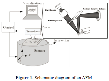
The conductive cantilever tip can act as a movable electrode that locally sets an electric stimulus to the sample. The control of the tip-sample distance sets the range at which the stimuli can be applied, and the value of voltage controls the field's intensity and polarization.
2.2. Anodic oxidation
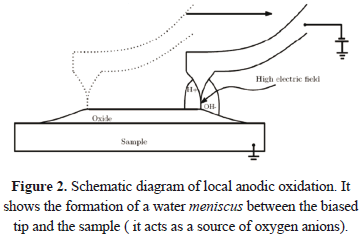
Anodic oxidation is an electrochemical process in which an oxide layer is generated on top of a substrate by attracting OH- ions near the surface. The localized prefix comes from the SPM technique used to generate the oxide layer, since the microscope's tip has a nanometer order radius and the oxidation can be performed in a similarly-sized area.
Local anodic oxidation takes place when a negatively polarized conductive tip is placed at close range of a grounded sample. The high electric field created around the sharp tip, causes the breakage of water molecules near the interface into ions H+, OH- and O-. The OH- and O- ions are then pushed away from the biased tip and forced into contact with the samples surface [12] (see Figure 2).
2.3. Methodology
The experiments were conducted on a silicon (100) substrate since this material is very commonly used in the microelectronics industry and MEMS device production. Initially, the samples were cleaned with an ultrasonic bath in isopropyl alcohol and acetone for 15 min. They were grounded using a copper wire attached with a conductive clip on the AFM's sample holder.
The AFM was a MFP3D-Bio by Asylum Research, Santa Barbara (USA). The probe was a silicon cantilever coated with platinum with a tip radious of 28nm. Its spring constant was 2 N/m and its nominal resonant frequency was 70 kHz (Olympus AC240TM). A set of 20 oxide lines were fabricated using a schematic process as illustrated in Figure 2.
3. RESULTS
Figures 3 and 4 illustrate the oxide lines fabricated on a Silicon (100) substrate following the process described above. From left to right, the patterns represent six different scanning speeds at which they were created, while vertically they represent five different fixed voltages.
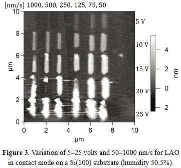
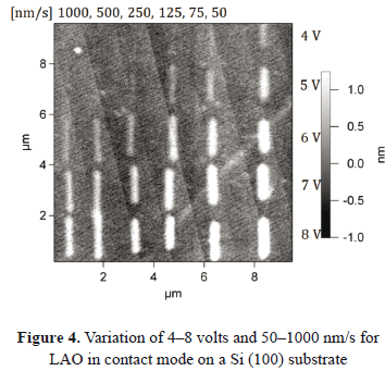
The figures show that the optimum fabrication of oxide nanostructures is within the range of 5–15 volts. Further analysis showed that the oxide nano-patterns have a logarithmic increase of width with voltage, whereas they have a linear increase of height, as shown in Figures 5 and 6. The width increased inversely proportional to the scanning speed, as shown in Figure 7. The higher the scanning speed, the shorter time the sample is influenced by the biased tip, limiting the control over the oxide patterns height and width.
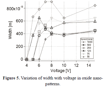
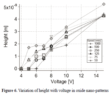
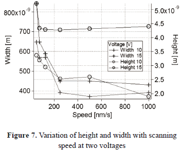
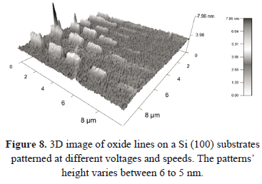
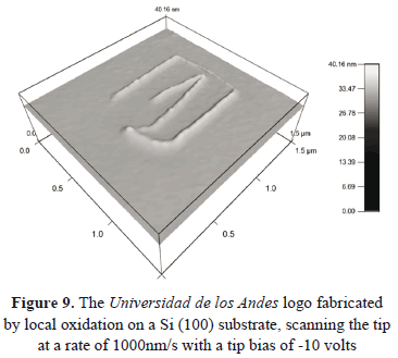
Figure 8 illustrates a 3D image of the oxide lines presented in Figure 4, and it shows the accuracy and power of this technique. A more complex patterning is also achievable through LAO, as presented in Figure 9.
4. CONCLUSIONS
This paper has demonstrated the characterization of oxide nano-patterns fabricated using LAO on an AFM. We have analyzed voltage and scanning speed and have rendered graphics describing the oxide patterns' size achieved with a particular set of parameters, at stable environmental conditions.
At high voltages (>15 V) and the scanning speeds analyzed, discharge effects appear on the formed oxide leaving discrete ridges in the pattern. When applying high voltages to a nanometer-scaled tip, the locally concentrated electric field can exceed the SiO2 breakdown. Along the patterned lines the irregularity of the bumps impedes the determination of width and height. From these results, LAO could provide a way for locally studying electrical discharge at a nanoscale.
In addition, the precise control of the aspect ratio in oxide lines will be a key factor in applications such as a mask for mass fabrication and lithography processes for the semiconductor industry. The LAO technique based on AFM has the unique capacity of allowing visualization immediately after generating the oxide patterns.
ACKNOWLEDGEMENTS
This work was supported by the Vicerrectoría de Investigaciones of Universidad de los Andes. Authors thank the clean room and the Microscopy Center at Universidad de los Andes for providing access to the Facilities and also Martin Espitia for his help.
REFERENCES
[1] Binnig, G. and Rohrer, H., "Scanning tunneling microscopyfrom birth to adolescence," vol. 59, P. 615, 1987. [ Links ]
[2] Shen, Z.Y., Hou, S. M., Sun, H., Zhao, X. Y. and Xue, Z. Q., Local oxidation of titanium thin films using an atomic force microscope under static and pulsed voltages. Journal of Physics D-Applied Physics, vol. 37(9), pp. 1357-1361, 2004. [ Links ]
[3] Fang, T. H., Wang, T. H. and Wu, K. T., Local oxidation of titanium films by non-contact atomic force microscopy. Microelectronic Engineering, vol. 85 (7), pp. 1616-1623, 2008. [ Links ]
[4] Jiao, N. D., Wang, Y. C., Xi, N. and Dong, Z. L., AFM based anodic oxidation and its application to oxidative cutting and welding of CNT. Science in China Series E-Technological Sciences, vol. 52(11), pp. 3149-3157, 2009. [ Links ]
[5] Garcia, R., Calleja, M. and Perez, F., Local oxidation of silicon surfaces by dynamic force microscopy: Nanofabrication and water bridge formation. Applied Physics Letters, vol. 72 (18), pp. 2295-2297, 1998. [ Links ]
[6] Park, C. H., Bae, S. and Lee, H., Nano-oxidation of Si using ac modulation in atomic force microscope lithography. Colloids and Surfaces a-Physicochemical and Engineering Aspects. vol. 284, pp. 552-555, 2006. [ Links ]
[7] Martinez, R. V., Martinez, J. and Garcia, R., Silicon nanowire circuits fabricated by AFM oxidation nanolithography. Nanotechnology, vol. 21 (24), 2010. [ Links ]
[8] Okada, Y., Amano, S., Kawabe, M., Shimbo, B. N. and Harris, Jr. J., Atomic force microscope nanoscale lithography for single-electron device applications. 1998, pp. 577-580. [ Links ]
[9] Keyser, U. F., Schumacher, H. W., Zeitler, U., Haug, R. J. and Eberl, K., Fabrication of a single-electron transistor by current-controlled local oxidation of a two-dimensional electron system. Applied Physics Letters, vol. 76, (4), pp. 457-459, 2000. [ Links ]
[10] Binnig, G. , Quate, C. F. and Gerber, Ch., Atomic Force Microscope. vol. 56, pp. 930, 1986. [ Links ]
[11] Bhushan, B., Springer Handbook of Nanotechnology. Bhushan, Springer-Verlag, Heidelberg, Germany, third edition.2010. [ Links ]
[12] Davis, Z. J., Abadal, G., Hansen, O., Borisé, X., Barniol, N., Pérez, F. and Boisen, A., AFM lithography of aluminum for fabrication of nanomechanical systems. Ultramicroscopy, vol. 97, (1-4), pp. 467-472, 2003. [ Links ]
