


 English (pdf)
 Article in xml format
 Article references
 Send this article by e-mail
 Cited by SciELO
  Cited by Google
  Similars in
SciELO
Similars in
SciELO  Similars in Google
 Permalink
1. Introduction
In 2004, Andre Geim and Konstantin Novoselov discovered, isolated, and characterized graphene. Progress on the research on its physical properties has been made since then. It is known that graphene is an sp2-bonded allotrope of carbon with a hexagonal two-dimensional lattice in which one carbon atom forms each vertex; it is the basic structural element of other allotropes, including graphite, charcoal, carbon nanotubes, and fullerenes. The two-dimensional lattice of graphene gives it its physical properties, such as its electronic band structure, which provides it with the effect of linear dispersion for charge carriers, high carrier mobility, massless Dirac fermions, and the anomalous quantum Hall effect (QHE) [1-8], which explains the quantum Hall plateau series for monolayer and bilayer graphene.
Another important physical property of graphene is its thermal conductivity value, which is above 2000 Wm-1K-1. This value allows it to induce a high thermoelectric voltage as a response to different temperatures. The measurement of voltage per Kelvin makes it possible to calculate the Seebeck coefficient (SC) of graphene. The Seebeck effect has been used in the generation of electricity and the measurement of temperature and as a temperature control. Nevertheless, there are few specific studies on this effect in graphene. For instance, Li et al. studied the dependence of the SC of this material on the number of layers. These authors reported a high Seebeck coefficient and gas-flow-induced voltage in multilayer graphene [9]. This paper presents the measurement of sheet resistance and the Seebeck coefficient in multilayer bare graphene and graphene covered with Ag nanoparticles.
In addition, according to recent research graphene exhibits linear non-saturated magnetoresistance (MR) that changes up to 100% [10]. This magnetic property potentially allows graphene to be used as a magnetic sensor [11,12]. MR is understood as the change of the electrical resistance as a function of the applied external magnetic field divided by the resistance at zero magnetic field.
There are few articles on MR in pristine graphene. However, for doped graphene the MR has reached values of up to 90,000% for an applied magnetic field of 9 T at 300 K in few-layer graphene/boron-nitride heterostructures [13].
It is known that metallic nanoparticles modify the structural and electronic properties of graphene, changes that could be used in electrical applications. Therefore, in this article the MR in bare graphene and in graphene covered with Ag nanoparticles is measured.
2. Experimental method
The graphene was grown on 25-µm-thick copper sheets (99.8%), which were degreased with acetone. The native oxides on its surface were eliminated with acetic acid and then the sheets were dried with nitrogen. Subsequently, the substrate was placed in a furnace to produce air oxidation in order to form Cu2O and CuO oxides. This process aimed to eliminate carbon residues, which can generate nucleation sites, inhibit the growth, decrease the quality of crystalline graphene, or promote the formation of several layers of graphene. In addition, the thermal treatment aimed to reduce the number of nucleation sites since a single nucleus was enough to initiate the growth of monocrystalline graphene.
The growth of graphene films was carried out through the chemical vapor phase deposition (CVD) process. The annealing treatment started with a first heating ramp that increased the temperature to 950 °C. Once this temperature was reached, it was increased to 1025 °C for 20 minutes and then for 1 hour. The process of thermal treatment was performed in an H2 atmosphere. The increased temperature decomposed the copper oxides by increasing the partial pressure of oxygen in the CVD chamber. The oxygen released reacts with the residual carbon on the copper surface to form carbon dioxide and carbon monoxide. In this way, the nucleation density and the growth of large graphene islands were considerably reduced. With the copper surface free of oxygen and carbon, the graphene growth stage began. With the same hydrogen atmosphere, the furnace was cooled to 910 °C. Methane was introduced to produce the graphene. At this stage of the process, copper was able to catalyze the decomposition of CH4 and to favor the formation of carbon atoms on the copper surface. Finally, the chamber was cooled with the two gases, hydrogen (103 sccm) and methane (10 sccm), to a 500 ºC for 1 hour and 30 min. The graphene produced on copper was transferred onto glass substrates. In this process, the graphene-copper sample was placed on a holder of a spinner and a drop of organic material (PMMA) dissolved in anisole was put on the surface. The spinner was programmed with a speed of 1500 rpm, which produces a thin film of PMMA on the surface. Subsequently, a solution of the copper was prepared by adding 2.8 M FeCl3 in 1.3 M HCl and heated at 40 ºC for 5 minutes. In the final part of this process, the FeCl3 solution was eliminated with distilled water and HCl (10% solution).
Ag nanoparticles (NPs) were deposited by using a sputtering-based cluster source (from Mantis Deposition Ltd.); this equipment is described in [14]. The NPs were deposited at 200 W for 15 and 30 s. These nanoparticles were deposited on graphene after of the transfer process.
The chemical composition was evaluated through Raman spectroscopy by using an argon laser with a wavelength of 488 nm and power between 22 and 120 mW with a Jobin Yvon HR- 460 monochromator equipped with a CCD camera. The resistance sheet of the bare and covered graphene was measured by using the van der Paw method with eq. (1):

where R1 and R2 are resistance measurements interchanging the current and the voltage electrodes and f is a constant with a value near one.
The Seebeck coefficient (SC) of the graphene was measured through a differential heating of 10 ºC of the sample, produced by two electrical resistances with an AC supply of 60 W. The SC is calculated by the relation ΔV/ΔT.
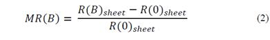
The magnetoresistance (MR) was measured using a Hall system equipped with a variable voltage supply (0-30 V), a current supply (0-1×10⁻³ A), and an electromagnet (0-0.5 T). The value of MR was evaluated by using eq. (2):
To measure MR, Ti/Au electrical contacts were deposited through sputtering under the following conditions: The Ti electrode was deposited with pressure of 1 Pa, power of 20 W and dc potential difference of 232 V, current of 0.8 A, and time of 5 minutes. The Au electrode was deposited with pressure of 1 Pa, power of 20 W and dc potential difference of 400 V, current of 0.05 A, and time of 50 minutes. The thickness of the electrodes was 1 µm.
3. Results and discussion
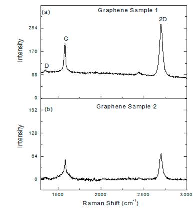
The effect on the morphology of the graphene caused by the transference process was analyzed through the Raman technique. Figs. 1a and 1b show the Raman spectra of two graphene samples.
Source: The Authors.
Figure 1. Raman spectra of graphene deposited on copper through the CVD method and transferred on glass. (a) Sample 1 used to measure Seebeck coefficient and (b) sample used to measure Magnetoresistance.
The spectra allowed the identification of D, G, and 2D Raman peaks located at 1,348.89, 1,582.55, and 2,695.22 cm-1, respectively. In the two samples, the D peaks had low intensity, while the intensity ratio I(G)/I(2D) was 0.5 in sample 1 and 0.7 in sample 2. These intensity ratios have been shown to be related to the number of layers of the graphene. For instance, according to Graf et al. [15] the G ratio at 2D ranged from 0.25 (monolayers) to 0.7 (6 layers). Therefore, if the results presented herein are compared with those in [15], sample 1 will have two layers and sample 2, six layers.
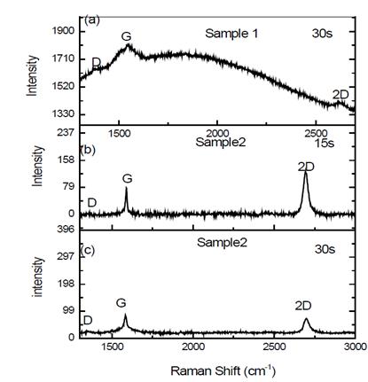
Fig. 2 shows the effect of Ag NPs on the graphene structure. Sample 1, after having been covered for 30 s, shows a wide Raman spectrum in which the D peak was located at 1,359 cm-1 and the G and 2D peaks were located at 1,547.23 and 2,614.28 cm-1, respectively. The ratio between the intensities of G and 2D peaks was approximately 3:1. The shape of the peaks suggests a superposition of multiple Loerentzian functions. Additionally, it is important to note that in this sample there were shifts in the positions of G and 2D peaks, which shift towards lower energies. These changes were reported by Graf et al. [15], who found that the G peak was located at 1,585 cm-1 in monolayers and shifted towards lower energies when the number of layers increased. The changes in the energy are more pronounced in the results presented herein, possibly due to Ag nanoparticles
Source: The Authors.
Figure 2. Raman spectra of graphene deposited on copper through the CVD method and transferred on glass. (a) Sample 1 with Ag NPs deposited for 30 s, (b) sample 2 with Ag NPs deposited for 15 s and (c) Sample 2 with Ag NPs deposited for 30 s.
After having deposited Ag NPs for 15 s, the Raman analysis of samples 1(no is include) and 2 showed that G and 2D peaks had the same intensity ratio as the bare sample. After 30 s in sample 2, this same ratio was approximately 1 and both peaks had undergone a 6 cm-1 shift towards lower energies in relation to the bare sample. These results confirmed that the graphene-NP system has a multilayer structure.
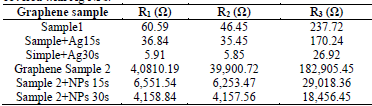
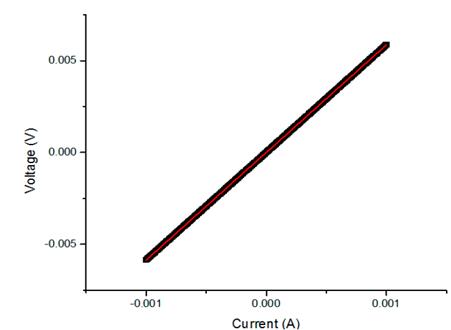
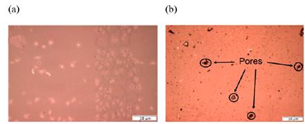
Fig. 3 shows the electrical representative behavior of the bare and covered graphene samples, and Table 1 summarizes the sheet resistance values obtained from the slope of these typical graphs. The results show that the sheet resistance of graphene of sample 2 is 769 times higher than the sheet resistance of graphene 1. These results can be explained by the optical micrographs in Fig. 4, which shows that the surface of sample 2 is more porous than that of sample 1. Since the porosity can open the electrical trajectory, the sample with more porosity has more resistance. Moreover, the results demonstrated that in both samples the resistance values decreased by a factor of 10 when they were covered with NPs. These results suggest that the NPs fill the pores and close the open electrical trajectories. In previous articles, the sheet resistance of graphene doped with TFSA polymer ranged between 0.5 and 5 K Ω.
Table 1. Values of sheet resistances for two samples of bare graphene and graphene covered with Ag NPs.
Source: The Authors.
Source: The Authors.
Figure 3. Voltage vs. current for a sample covered with Ag NP. The red line is the theoretical fit.
Source: The Authors.
Figure 4. Micrographs of graphene deposited on copper through the CVD method and transferred on glass. (a) Sample 1 and (b) sample 2.
The authors suggest that the wide range of values of sheet resistance could be attributed to differences in growth parameters as well as defects induced during the transfer process [16].
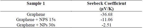
For sample 1, the Seebeck coefficient (SC) was measured. Table 2 summarizes the values obtained in the bare and the covered samples. The sign of the SC shows that the electrical carriers are negative. Additionally, the SC of Graphene decreased in absolute value when NPs were deposited on its surface, i.e., when the number of layers increased. The Seebeck coefficient of graphene was caused by the interplay of the band structure, defects or disorder induced by scattering, the temperature, and intense magnetic fields through Landau quantization [17]. Therefore, the decrease in the SC obtained in the graphene sample can be explained as follows: the greater the number of layers, the greater the decrease in defects and scattering. In addition, it is important to mention that the value of SC reported for two layers was 32.50 µV/K [9]; this value differed by approximately 12% with the one presented in this article.
Table 2. Seebeck coefficient of bare bilayer graphene and graphene covered with Ag NPs.
Source: The Authors.
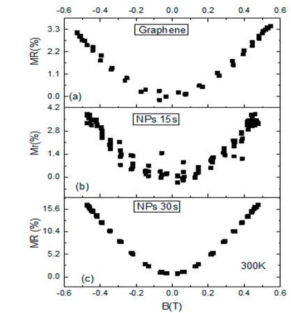
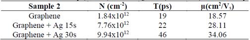
For sample 2, the magnetoresistance (MR) was measured at room temperature. Fig. 5 shows the behavior of the MR as a function of the magnetic field; for low magnetic intensity, this behavior is described by the Lorentz magnetoresistance, developed by M. Kohler: MR ∼ (ωcτ)2, with ωc (e/m B) the cyclotron frequency, and τ the scattering time [18].
Source: The Authors.
Figure 5. Magnetoresistance of graphene measured at room temperature. (a Pristine, (b) covered with Ag NPs for 15 s, and (c) covered with Ag NPs for 30 s.
The results showed that the MR of graphene increased from 0.0% to 3.0%, while it increased to 3.8% when covered with NPs for 15 s. An important change occurred in the MR when the graphene was covered with NPs for 30 s, since it increased to 16.6%. The increase in the MR of graphene covered with NPs can be explained by considering that the scattering time is increased when NPs were deposited (see Table 3), because dispersive phenomena produced within the imperfections of the graphene lattice (pores and contaminants) decreases. Since in covered graphene the sheet resistance decreased by a factor of ten while the carrier density increased by more than a factor of five in relation to bare graphene, this caused their mobility to be greater than that of bare graphene. These results are different from those found in graphene doped with nitrogen and TFSA polymer [16, 19]. As demonstrated in those articles, the MR of graphene decreased when it was doped. The MR behavior was different because the resistance sheet of the graphene doped with nitrogen was between 7 and 36 kΩ, and that doped with polymer was between 0.5 and 5 kΩ.
4. Conclusions
Multilayer graphene was grown through the CVD method. It was covered with Ag NPs, and the Seebeck coefficient and the magnetoresistance were measured. The results show that the thermoelectric and magnetic properties strongly depend on the surface morphology, since samples with larger defects have a large sheet resistance, low dispersive time, and low electrical mobility. These parameters define the above-mentioned physical properties.

