


 English (pdf)
 Article in xml format
 Article references
 Send this article by e-mail
 Cited by SciELO
  Cited by Google
  Similars in
SciELO
Similars in
SciELO  Similars in Google
 Permalink
1. Introduction
Currently, the photovoltaic technologies focus on the development of new materials which allow reducing the electric dependence and promote a low environmental impact, which represents the main challenge in the progress of solar technology, principally concentrated in the use of non-rare elements, low toxicity and the possibility of production at industrial level [1-5]. Recent studies in this field have been pointed that synthesis and characterization of chalcopyrite compounds like CuInS2 (CIS), AgInS2 (AIS), kesterite Cu2ZnSnS4 (CZTS) and stannite Cu2FeSnS4 (CFTS) materials have been shown excellent performance on photovoltaic technologies (PV) since the stannite/kesterite structure is based on non-rare, abundant elements in the earth surface and also exhibit an effective band-gap semiconductor behavior with values around 1.5 eV [6-8].
The photovoltaic cell efficiency (abbreviate PCE) of a p-type CZTS thin-film system (abbreviate TFSC) has achieved values around 12.6%, which makes that its fabrication process be particularly challenging to reach comparable values to other devices like the polycrystalline silicon [9,10]. However in the case of CZTS materials and derived structures, due the similar atomic radius between Cu and Zn have, is clear an intermixing phenomena in the crystal lattice that evidence multiple structural defects and electrostatic potential fluctuations due to the concentration of CuZn+ZnCu sites, which deteriorates the solar cell efficiency [11-13]. As result, it is essential to find alternatives to kesterite structure synthesis, as well as an opportunity to improve the relationship between Cu or Zn in the lattice with some other elements, which become an exciting alternative to decrease the optical band-gap (1.28-1.50 eV) and the optical absorption coefficients (> 104 cm-1), in CZTS materials [10-12,14,15]. In this sense, although Fe is more soluble in the lattice and produces an increase in conductivity, according to Vanalakar et al. [13], the Cu2FeSnS4 material shows an Sn-S polyhedral structure that promotes the replacement of Zn by Fe, which may change the polarizability, improving the surface morphology and the concentration of intrinsic defects in a very effective way, depending on the grain size and defects concentration, reducing the carrier recombination at grain boundaries, contributing to conversion efficiency when the material is used as absorber layer in the design of solar cells. It is clear that the obtention of CFTS materials by means of non-conventional routes enable the development of suitable properties characterized by a high control of homogeneity, average crystal size through a facile and low-cost procedure.
Even though CFTS-based solar cells have a relevant photoconversion efficiency [15], only since 1967, about 90 papers on CFTS thin films and nanocrystalline structures have been published according to Vanalakar et al. [10,13]. Several procedures have been used to date, including hydro and solvothermal, hot injection, microwave aided, and liquid reflux methods, the reason why this route is a well-known and efficient method to design new materials at low cost [13,16,17].
In this context, it is clear that current work focuses on the synthesis, characterization and assembly of a solar cell based on a CFTS stannite system, using a one-step hydrothermal reaction, starting from corresponding dissolutions metal salts. The work will permit the identification of the optimal reaction time, and its dependence is given the thermal treatment, thus in order to get the principal crystalline structure of CFTS with some apparent semiconductor properties, removing the conventional sulfurization process and contributing to reducing the production costs of photovoltaic materials based on stannite structures where further thermal treatments are required.
2. Methodology
2.1. Hydrothermal synthesis
The three CFTS materials were obtained from metal cation dissolutions, which were prepared to start from corresponding nitrates of Cu(NO3)2·6H2O, Fe(NO3)3·9H2O, anhydrous tin chloride SnCl2, and thiourea (abbreviated TU) as a sulfur source in deionized water Milli-Q (18 M(.cm). The metal salts dissolutions were standardized at 1.0 molL-1 concentration, and the TU was added in solid form into a Teflon vessel autoclave according to its solubility constants. The resultant mixture in stoichiometric quantities of each metal cation and TU were subjected to magnetic stirring (250 rpm) for 30 min at room temperature until homogenization. After this, the autoclave was sealed and placed in an electric convection oven for different times (12, 24, and 48 hours) at 573 K. At the end of each process, the autoclave was cooled, and the CFTS materials in each case were washed several times in absolute ethanol to remove unwanted products. The obtained materials at 12, 24, and 48 hours were dried at 343 K in an electric oven before characterization.
2.2. Materials characterization
According to the suggested method, the obtained materials the structural, morphologic, and optoelectronic properties were evaluated. The structural analysis by XRD analysis using a PANalytical X´pert PRO-MPD equipment with Ultra-fast X'Celerator in a Bragg-Brentano configuration, using the Cu radiation Kα (λ= 1.54186 Å) between 10° and 90°. The Raman vibrational spectroscopy measures were carried out in an NRS-3100 Raman spectrophotometer with simple monochromator 600, 1/mm grid, UMPLFL 20 x BS/DM 785 nm lens, and a 10.4 mW laser power. The morphological analysis was carried out by scanning electron microscopy (SEM) using an LEO 440 (Leica-Zeis) microscope with an electron gun and an acceleration voltage of 1-30 kV with an X-ray dispersion spectrometer. The transmission electron microscopy (TEM) analysis was carried out in a JEOL 2100 microscope with an acceleration voltage of 200 kV with a CCD high-resolution image chamber using Au coating.
The electrical efficiency of a photovoltaic cell assembled using the CFTS 48h material was done using a precision micro-diamond scriber MR200 OEG equipment in which a precision tracing tool of a diamond tip tool and an optical system of positioning was used to create the microcells of 0.090 cm2. The cell was tested in a Sun 3000 class AAA solar simulator, Abet Technology, equipped with standard lighting conditions AM 1.5 and 100 mW/cm2. The electric parameters at open-circuit voltage (Voc), short circuit current (Isc), fill factor (FF), and efficiency was determined from the data provided by the simulator.
2.3. Construction of photovoltaic cell
With the use of 0.5 g of CFTS 48h sample, it was possible to produce a grounded mixture using 5 mL of DMSO (Merck 99.9%), which was stirring for 30 min at room temperature. The solid was dissolved. It is kept stirring until the obtention of a homogeneous solution serves to deposit the material as a film, using the spin coating technique over a commercial substrate coated with metallic molybdenum 20x20 mm2. The substrate was previously washed with isopropanol and activated under thermal treatment at 323 K in an electric oven for 20 min. The spin coating method allows the deposition of 10 layers of material at 2000 rpm for 20 seconds, and in each deposit, the drying was carried out on a hot plate at 423 K for 5 minutes in each cycle. The substrate configuration was (Mo/CFTS48/CdS/i-ZnO/ITO), where the CdS and i-ZnO layers were deposited by chemical bath deposition (CBD), and the ITO layer was sputtered in a DC magnetron sputtering equipment. The layers of CdS and i-ZnO were applied with an approximate thickness of 50 and 400 nm, respectively, and the ITO layer with a thickness of 450 nm, to obtain the I−V plots:
3. Results
3.1. Structural analysis by X-ray diffraction
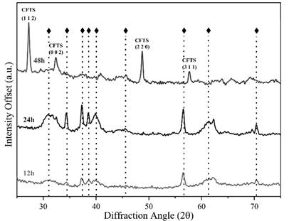
The Diffraction patterns of solids shown in Fig. 1, confirm the obtention of a CFTS structure in case of 48 hours material, with secondary phases (() related to the synthesis procedure in case of CFTS 12 and CFTS 24. Also, it is clear the ordering of the preferential lattice patterns of the structure as well as an increase in the intensity of the signals according to the rise of the temperature.
Source: Own source
Figure 1 XRD patterns of the CFTS polycrystalline materials were obtained at 12h, 24h, and 48h by a hydrothermal procedure.
The diffraction patterns were analyzed through X'Pert HighScore software using the JCPDS/PDF databases; the results confirm the presence of Cu4Fe2Sn2S8 material, identified with JCPDS 70-4373, tetragonal crystalline system I-42m space group, cell parameters a=5.46, b=5.46, and c=10.72 Å, α, β and γ=90 ° with a cell volume 320×106 pm3 in CFTS 12 and CFTS 24 solids. These parameters were correlated with the obtained material by indexing each intense signal related to the (1 0 3) and (2 2 1) facets to 34.91 and 56.64 2𝛉 degrees, respectively. According to the diffraction patterns, the obtention of a Stannite crystalline phase was achieved as following previous results [18,19]. In identifying process, the stannite crystal structure exhibit secondary phases derived from the hydrothermal synthesis procedure at low temperature, such as SnS2, CuS, FeS2, and ZnS.
On the contrary, in the CFTS 48 material, the crystalline structure was consistent with the JCPDS 44-1476, tetragonal crystalline system I-42m space group, cell parameters a=5.4501, c=10.7390.72 Å, α, β and γ=90 ° with a cell volume 319×106 pm3, along main diffraction signals located at 27.09, 32.78, 48.86 and 57.61° 2𝛉 of (1 1 2), (0 0 2), (2 2 0) and (3 1 1) facets respectively; being clear that the increase in the reaction time, leads to a significant consolidation of the CFTS phase. Such results provide strong evidence of low thermodynamic stability of secondary phases under proposed synthesis conditions, leading to the obtention of a polycrystalline sample with a high lattice-match concerning desired characteristics.
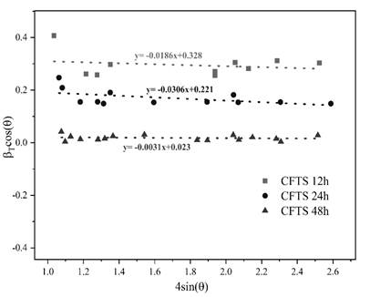
Using the Williamson-Hall plot method (Fig 2) to estimate the average crystal size of the obtained materials with 5.16 nm, 7.68 nm, and 73.68 nm at 12, 24, and 48h each one was clear that the reaction time has a direct influence on the crystal size due to the strain constant slightly decreases, thus enhance the stabilization of the lattice ordering into the polycrystalline structure, providing a high crystallinity shown in the 48h reaction time diffractogram (Fig 1) of the obtained material [16].
Source: Own source
Figure 2 Williamsom-Hall plot of the CFTS polycrystalline materials obtained at 12h, 24h, and 48h.
Even though the XRD analysis is the most frequent tool used for structural determination, this technique cannot distinguish between some of the additional signals that could be present and related to some additional phases that can be derived from the proposed synthesis procedure. In fact, that is the main reason for which the X-ray diffraction pattern of CFTS (JCPDS 70-43-47) is quite similar to FeS (JCPDS 23-1123) and Cu3SnS4 (JCPDS 33-0501). Given the above, the knowledge and identification of each of the crystal phases present in the crystal lattice is an essential parameter in order to clarify the electronic properties due to the structural and vibrational properties of the material, in which the vibrational identification of all crystal components by Raman spectroscopy provides a more reliable and clear differentiation of the crystal structures into the obtained materials [20].
3.2. Vibrational analysis by Raman spectroscopy
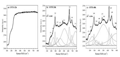
From vibrational analysis shown in Fig 3, it is possible to confirm the obtaining of the polycrystalline CFTS materials with a stannite crystal structure and its corresponding space group (I-42m), which, when contrasted with the Bilbao Crystallographic Server, reveals a correlation with the Mülliken notation (D2d) according to the punctual group notation, where the polarization tensor that involves active bands in Raman spectroscopy can be described as ( = 2A1(2B1(4B2(LO/TO)(6E(LO/TO) in accordance with X. Fontané and others, [21-24]. In this sense, the correlation between the structural properties with the vibrational behavior of the system is framed.
Source: Own source
Figure 3 Raman Non-linear fit profile (NLFP) with Lorentzian functions of the CFTS polycrystalline materials obtained at a. 12h, b. 24h and c. 48h.
Given the active and expected bands by Raman spectroscopy, the A1 as the principal vibrational mode is expected to exhibit two strong signals which involve cation displacing movements, as has been observed in Chalcopyrite structures [24,25]. Polarization tensor also shows B2 and E actives modes in Raman and IR, which is also a LO-TO splitting due to the polar nature [24]. Fig. 3b, 3c showed non-linear peak profile fitting using Lorentzian functions for the obtained solids, between 150 and 800 cm-1 where the strongest signals occur, having found that as the reaction time increases, the intensity of the related peaks grows mainly in the CFTS 24 and CFTS 48 samples.
Fig. 3a shows no evidence of a significant crystal lattice ordering that allows the vibrational transitions of a crystalline material to be produced. According to the fitting of the experimental data with Lorentzian functions shown in Fig. 3a and 3b, has allowed finding characteristic predominant peaks at 290 cm-1 and 289 cm-1 which are attributed to the all one-dimensional symmetric cations which moves towards x-axis positive values according to A1 vibrational mode from stannite structure [24,25]. Also, weaker contributions were found at 250 and 251 cm-1 endorsed as one-dimensional asymmetric B2 vibrational mode where half of the Cu atoms move toward positive values of the z-axis (perpendicular to the Cu-Zn plane). However, the other half moves toward negative values of the z-axis, while Zn and Sn atoms remain stationary. However, peaks at 341 and 344 cm-1 move toward xy as a typical two-dimensional representation of E vibrational mode for stannite crystal lattice [24,26]. Peak fitting profile of data also reveals additional phases related to the hydrothermal synthesis procedure where SnS2 (184 and 175 cm-1)[26-29], CuS (473 cm-1)[30], and FeS2 (513 cm-1) [31,32] through the association of a vibrational mode A1g at where Sn-S, Cu-S, Fe-S atoms move evenly toward the inversion center, one-dimensional vibration peaks found at 626 and 628 cm-1 rated to characteristically A1 vibrational mode of ZnS [33,34].
Thus, it has been clear that vibrational analysis allows to not only make a clear identification of every additional phase present onto the polycrystalline structure but also confirm due to the intense Raman peak in the spectra that obtained material at 48h shows significant improvements in crystallinity order of the polycrystallinity of the Stannite-type structure thorough the slight contractions on the lattice parameter observed within the Williamson-Hall plot and XRD results.
3.3. Morphological analysis by transmission electron microscopy (TEM)
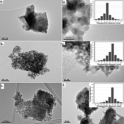
The TEM analysis of samples exhibits the presence of nanocrystallite clusters with heterogenous composition and small grain boundaries, as shown in Fig. 4. The average crystallite size of CFTS nanoparticles is expected to be approximately 6, 8, and 74 nm as reaction time increase by 12h to 48h, respectively, as has been corroborated by K. Mokurala et al. [35] through the analysis of W-H plots.
Source: Own source
Figure 4 TEM images and particle size distribution of the CFTS polycrystalline materials obtained at a, b. 12h, c, d. 24h and e, f. 48h using the IMAGE-J software.
In the transmission electron microscopy images, was evident the obtention of nanoparticle structures of CFTS, with crystal sizes associated with XRD results. The images of Fig 4 reveals agglomerated nanoparticles derived from high surface area according to with synthesis method except in sample obtained at 48 h, in which the crystalline size of the material is around 70-80 nm; these results were obtained with a population of 100 particles per image using the IMAGE-J software. In general, the particles are homogeneously distributed, and such results are consistent with previous results [36].
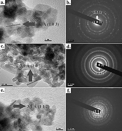
The HR-TEM and SAED analysis (Fig 5) shows dispersed nanocrystals with an average size around 7-8 nm for samples obtained at 12 and 24 hours; however, for the sample obtained at 48 h, the crystallite size is around 75 nm. The images processed by the IMAGE-J software reveal an excellent crystallinity level of all samples and interplanar d-spacing along (1 0 3) facet of 2.7-3.1Å for CFTS 24 and CFTS 48 in agreement with results of Jiang et al., [4], besides the particle size expected by the W-H plot. The further analysis evaluated by means SAED patterns shows structures conformed by rings of main diffraction signals with dominant spots, mainly in samples obtained at long time reaction, indicating a polycrystalline nature of the materials. The selected area electron diffraction (SAED) pattern of Fig. 5 matched with the stannite structure of CFTS.
Source: Own source
Figure 5 HR-TEM and SAED pattern images of the CFTS polycrystalline materials obtained a, b. 12h, c, d. 24h and e, f. 48h with its corresponding d-spacings.
The grain sizes of materials are one of the essential factors affecting the performance of polycrystalline solar cells, due to large grain size could increase the carrier diffusion length and reduce the carrier recombination at grain boundaries, contributing to conversion efficiency solar energy [4]. In general, the dispersed nanocrystals are consistent with a tetragonal crystalline system I-42m, as has been previously established [35,37,38], confirming the effectiveness of the proposed method to obtain the proposed materials under long reaction time conditions.
3.4. Optical properties measured by UV-Vis absorption spectroscopy
The optical properties measurements were carried out through absorption spectra in UV-Vis spectroscopy, considering that the molar absorptivity coefficient of the obtained materials given the absorption data of each of these is more significant than 104cm-4 in the visible region, then, the semiconductor performance is established as direct allowed transitions following what is expected for CFTS/CZTSe structures. In the direct transition semiconductor, the optical energy bandgap (Eopt) and the optical absorption coefficient (α) are related by the eq. (1) [39,40] .
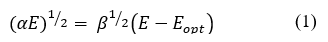
Where α is the absorption coefficient, β is the optical density of state and E is the photon energy. Therefore, the optical bandgap can be obtained by extrapolating the tangential line to the photon energy (E=hυ) axis in the plot of (αhυ)2 versus photon energy (hυ) [41,42]. The UV-vis absorption measurements thorough the band-gap calculation by the Tauc method (Fig 6) show that as the reaction time increases, the bandgap decreases from 3.909 to 3.709 eV, suggesting the obtaining of a disordered Stannite phase due to the increased bang-gap values given the arrangement between the Cu/Fe atoms in the polycrystalline material lattice [43]. Although the band-gap values for Stannite-type materials are reported between 1.5-2.0eV[44], hence the additional phases derived from the synthesis process contribute significantly to the increase in the band-gap of the polycrystalline system. The lattice ordering into the polycrystalline obtained materials structures given by the W-H plot (Fig. 2) suggests that as the stabilization due to the total broadening of the crystal lattice increases, the band-gap decreases.
Source: Own source
Figure 6 a. Tauc plot for Bang-Gap calculation from b. absorption spectra of the CFTS polycrystalline obtained materials at 12h, 24h, and 48h.
It is clear that structural analysis acquired by XRD, Raman vibrational analysis, and TEM indicates highly correlated properties of the obtained materials to the semiconducting performance of the CFTS polycrystalline material, which is significantly affected by the reaction time in the hydrothermal procedure [45].
3.5. Solid-state impedance spectroscopy
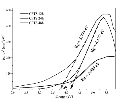
The results derived from impedance spectroscopy shown in Fig. 7, obtained at different temperatures from 298 to 573 K each 50 K, confirm a strong dependence of conductivity to the carrier transport concentration in CFTS samples obtained at different temperatures.
Source: Own source
Figure 7 Nyquist plots for CFTS samples at a. 12 h, b. 24 h, and c. 48 h from 298 to 573 K with different electrical resistance values.
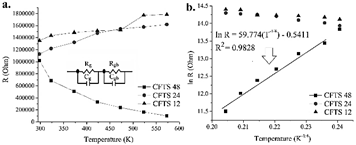
The impedance results allow obtaining information related to the electrical properties of the CFTS material and, in particular, of the processes involved with the charge carriers as a function of the frequency used in the measurements between 40 Hz and 1 MHz. The decrease of the values of impedance with increasing temperature and frequency is consistent with a behavior of the typical resistance coefficient in semiconductor materials, which only applies to the case of CFTS compounds obtained at 48 hours, since in the other cases (12 and 24 hours), it is clear that resistivity increases with temperature: the higher the temperature, the higher the resistivity, and therefore, the lower conductivity, which is consistent with a metallic behavior and present in alloys or compositions in which the purity of the desired phase is not optimal [46]. It is evident in all cases that in the low-frequency region, the values are very close to zero in all cases, with which the presence of polarization effects in the measurements made can be ruled out. In the case of the CFTS sample obtained at 48 hours, the reduction in impedance values decreases with increasing temperature, which indicates that the processes are thermo-dependent associated with Debye-type relaxation mechanisms, in which the graphs of Nyquist are fitted with an equivalent circuit model that determines the existence of impedances associated with grain limits (RgCg), which were evaluated using the Z-plot software, revealing that these become less capacitive and resistive due to the effect of temperature as shown in Fig. 8a.
Source: Own source
Figure 8 a. Grain resistance vs. temperature and b. Mott variable range hopping model in CFTS samples at different temperatures.
It is thus evident that in the case of CFTS 12h and CFTS 24h materials, the increase in temperature brings with it an increase in resistance from values of 1.35x10⁶ to 1.78x10⁶ ( and from 1.12x10⁶ to 1.61x10⁶ ( in each case, respectively. This behavior can be attributed to the presence of SnS2, CuS, FeS2, and ZnS compound in the phases achieved at 12 and 24 hours, which supports an alloy-like behavior as indicated in previous X-ray diffraction analyzes. In contrast, the decrease in resistance from 1.02x10⁶ ( at room temperature (298 K) to 9.84x10⁵ ( at 573 K for the CFTS 48h sample is attributed to a net semiconductor behavior and a decrease in grain boundary width, determining that there is a significant relationship with the grain limits driving mechanism linked to Mott's variable range jump model, in which the relationship ln(R/Ro) = (To/T)1/4 is applied. The model allows us to explain the prevalent conduction mechanism in this semiconductor material, establishing that at high temperatures, the charge carriers produce a random potential fluctuation attributed to the jumps that can occur between the active structural sites within a specific range of energies that are characterized by having certain activation energy values, which can be obtained from the slope of the straight line that is generated when graphing Mott's variable range jump model as indicated in Fig. 8b [47].
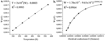
The analysis of the data of the Mott model allows to obtain the values of To, such as the slope of Fig. 8b, with which and making use of the expression for the calculation of the energy for the load carrier W = 0.25KBT0 1/4T3/4, thus the activation energy values for this process can be obtained, as indicated in Fig. 9a.
Source: Own source
Figure 9 a. Activation energies of grains and grains boundary as a function of temperature between room to 573 K, and b. Activation energy vs. electrical conductance G in CFTS 48 sample.
The calculated values of the activation energies allow obtaining the electrical characteristics of the material, being able to confirm the existence of thermally activated charge transfer processes, where the jumps of the charge carriers occur in the context of a potential well, according to Fatima et al. [48]. It is clear that the activation energy calculated for the CFTS 48 material is dependent on the electrical conductance values (G) up to a point where its behavior becomes asymptotic according to the trend shown, up to limit values of 0.00175 eV, which indicates that this process is subject to a mechanism that stabilizes near the maximum measurement temperature of 573 K, in accordance with an electronic type transfer process as indicated in the eq. (2):
These prevalent conduction mechanisms of electronic type are consistent with the adjustment of the equivalent circuit model provided by the Z-plot software of Fig. 8a; thus, Mott's variable range jump model determines that the conductance is attributed to a purely electronic load transfer phenomena rather than processes associated with the presence of vacancies in the crystal lattice, which requires a more significant energy input [49].
3.6. Electrical performance of CFTS 48 photovoltaic cell
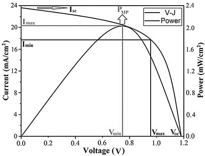
Fig. 10 shows the curve of the electrical characteristics of the photovoltaic cell assembled with the CFTS 48h material. The results show that the device exhibits an efficiency close to 2.15%, in an area of 0.090 cm2, where the open-circuit voltage (Voc) is located around 1.18 V with short-circuit current values (Isc) close to 23.6 mA/cm2, with e a fill factor closes to 60.42% is identified. Such value is associated with the eventual discontinuity of the layers of the CdS cell and i-ZnO-ITO, which generate a resistive effect under the deposition conditions developed in this paper.
Source: Own source
Figure 10 Multijunction cell device ensembled with the 48h CFTS photovoltaic material and its V-I curve and power diagram tested at room temperature.
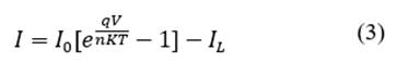
Analysis of the V-I curve of the solar cell under lighting conditions shifts the curve slightly towards the fourth quadrant where energy can be extracted, such that the current can be analyzed with eq. (3):
Where I L is the light current, so its effect on the characteristics of the current-voltage graph can be analyzed by the eq. (4):
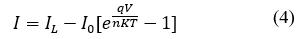
Since the -1 term in the previous equation can usually be neglected due to the exponential component being much more prominent, this suggests that the curve obtained has a maximum power identified as PMP, where the CFTS cell could be operated to generate the maximum output power, which is given at current values between 17.9 and 20.8 mA/cm2 and limit voltages between 0.75 and 0.94 V. Although the results of the photovoltaic characterization show that the efficiency is very low for this case, it is possible that under improved and controlled synthesis conditions with longer reaction times and temperatures, they allow consolidating a purer crystalline phase in order to improve the eventual application of these technologies to the design of more efficient solar panels.
4. Conclusions
It has been determined that the dependence of the reaction time at a constant temperature given the proposed synthesis procedure has an enormous impact on obtaining CFTS polycrystalline stannite type materials. From the structural properties analysis, the stabilization of the solid crystal lattice, given its total broadening, was evident by increasing the reaction time, confirming the obtaining of polymorphs derived from the synthesis procedure. Considering the above, it is clear then that the time reaction leads to a stabilization of the crystalline lattice, reducing the appearance of polymorphs and consequently modifies the optoelectronic and optical behavior of the obtained materials. Even rugged that materials with an apparent semiconductor behavior were obtained, the appearance of polymorphs fomented a dramatic reduction in its performance as an absorbent layer in a photovoltaic device.
Finally, the need to expand the research on this class of materials suits clear once the dependence of the reaction time has been confirmed, pushing the perspectives towards longer reaction times, seeking a proper stabilization and consolidation of the crystal lattice that eventually allows increasing the efficiency of high-performance photovoltaic devices.

