


 Inglés (pdf)
 Articulo en XML
 Referencias del artículo
 Enviar articulo por email
 Citado por SciELO
  Citado por Google
  Similares en
SciELO
Similares en
SciELO  Similares en Google
 Permalink
1. Introduction
One of the most important challenges facing humanity today is the reduction of pollution generated using fossil fuels. To meet this challenge, solar photovoltaic (PV) is a clean energy generation alternative, with very low levels of greenhouse gas emissions in operation and significant reduction of the levelized cost of electricity (LCOE). Between 2010 and 2020, the LCOE of PV plants was reduced by 85%, from 0.381 USD/kilowatt hour (kWh) to 0.057 USD/kWh in 2020 [1].
Historically, silicon has been the most widely used semiconductor in the photovoltaic industry due to abundantly available raw materials, stability and no apparent environmental health or safety issues. However, perovskite has several advantages over Si cells, as they are compatible with scalable printing fabrication methods and have a high absorption coefficient that facilitates the production of thin, light and even flexible devices [2]. These advantages make perovskite technology promising for niche markets such as: building integrated photovoltaics (BIPV), agrovoltaics, flexible devices, IoT, among others [2]. Recently, perovskite solar cells with an energy conversion efficiency (PCE) of 25.8% have been fabricated at laboratory scale, which is close to the maximum efficiency achieved with Si cells. But these highly efficient devices can only maintain 90% of their initial efficiency for 500 hours of illumination, which calls for research into strategies to increase temporal stability under real-world operating conditions.
Recent reports have shown that the decrease or replacement of organic cations (e.g., CH3NH3 + in MAPbI3 which is the most studied perovskite because of its simple composition and processability) by an inorganic cation such as Cs+ improves thermal stability [3]. Z. Li et al., developed a structure with 10% Cs+ ions (FA0.9Cs0.1PbI3), achieving an efficiency of 23.21% which maintains 80% of its initial efficiency after 500 h of continuous light soaking [4]. X. Zhu et al., incorporated 23% of Cs in the MA1-xCsxPbI3 structure, achieving a cell efficiency of 20.13% and the devices stored in the dark for one year decreased only 4.37% of the initial efficiency [5]. G. Tong et al., fabricated a totally inorganic perovskite with the Br-1 anion (CsPbBr3) and achieved a PCE of 10.91% which maintains 90% of initial PCE after 1000 h and 80% of initial PCE after 2000 h in conditions of 45% relative humidity and 100 °C [6]. Yixin Zhao et al., achieved a PCE of 19.03% in a device with the perovskite structure CsPbI3 which exhibited good photo-stability and retained 90% of their initial PCE after 500 h of continuous illumination [7]. Chunfu Zhang et al., fabricated a full inorganic perovskite with the structure CsPbI2Br, achieving a PCE of 19.3% which maintains 41.9% of its initial PCE even in deep water [8]. This research demonstrates the possibility of having perovskite solar cells with remarkable improvements in stability due to the incorporation of inorganic cations.
There are several ways to increase the stability of perovskites under different environmental conditions. One of them is to promote structural stability between the cations and anions that make up the ABX3 crystal. Goldschmidt tolerance factor (t) is a ratio that helps to calculate the preferential structure formed depending on the cations and anions used as shown in eq. (1) where R is the radius of each component in the structure. By tuning the t-factor it is possible to find the conditions for the structure to remain in the desired alpha-cubic phase for a long time (Fig. 1) [9].
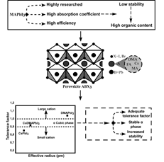
Source: own elaboration.
Figure 1 Schematic representation of stability increment by tuning the tolerance factor
In this work, a composition with a significant decrease in the organic component of the perovskite structure ((Cs1-xDMAx)Pb(Br1-xIx)3) was studied. A pure phase of this material with morphology suitable for device fabrication was achieved. Additionally, we demonstrated with x-ray diffraction (XRD) analysis that the stability of this composition is considerably higher than that of the MAPbI3 sample. Furthermore, this perovskite was integrated in an optoelectronic device obtaining a PCE of 7.93%. This paper is an extension of the work originally presented at Expo-engineering 2022 [10], which expanded the state of the art, methodology and analysis of results, especially morphological and structural characterization.
2. Materials and methods
2.1. Materials
N,N-dimethylformamide (DMF) from Sigma Aldrich, hydroiodic acid from Sigma Aldrich, PbI2 >99.99% from, CsI >99.99%, and PbBr2>99,998% from Alfa Aesar, dimethyl sulfoxide (DMSO) from Sigma Aldrich, SnCl2-2H2O from Sigma Aldrich, ITO glass, Silver 99%, Spiro-OMeTAD from 1-Material, Lithium salt from Sigma Aldrich, Co (III) TFSI Salt from great cell solar.
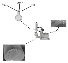
2.2. Synthesis of DMAPbI3
This phase is synthesized by the decomposition of DMF in the presence of an acid rich medium (HI), subsequently mixed with the lead precursor (PbI2). The reaction mechanism is shown in eq. (2), where DMF upon decomposition and mixing with the acid iodide produces DMAI [11]. Finally, DMAI when mixed with lead, forms the DMAPbI3 phase. The mixture contained 1:1 HI to DMF ratio, then PbI2 with a concentration of 1M was added, the solvent was slowly evaporated in a rotary evaporator for 6 h at 110°C, and faint yellow powders were collected. The summarized preparation process of this phase is shown in Fig. 2.

2.3. Synthesis of the perovskite precursor
The precursor of this perovskite was synthesized by mixing the DMAPbI3 phase obtained in the previous step with PbBr2 and CsI in DMF:DMSO 1:1.4. For this purpose, different molar ratios between the components were used to arrive at the purest possible phase. The ratios used were 1:1:2, 1.36:0.74:2, and 0.3:0.7:0.7 respectively, producing the phases Cs0.3DMA0.3Pb0.66Br0.66I1.66, Cs0.45DMA0.66 Pb0.7Br0.49 I2, and (Cs1-xDMAx)Pb(Br1-xIx)3 with x=0.3.
2.4. Solar cell fabrication
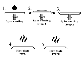
The solar cell was fabricated by spin coating, in which the ITO was coated layer by layer under different conditions. Initially, SnCl2-2H2O dissolved in isopropanol was deposited at a rate of 3000 rpm using the static method. Then, it was annealed at 180 °C for 1 h to obtain SnO2 used as the electron transport layer (ETL). Then, another SnO2 layer was deposited by chemical bath synthesis (CBD). Next, perovskite was deposited under different spin-coating conditions as shown in Table 1, followed by two stages of annealing at 70 and 170 °C, this deposition process is schematized in Fig. 3. Subsequently, Co and Li-doped Spiro-OMeOTAD was deposited to form the hole transport layer (HTL) of the solar cell by dynamic spin-coating at 4000 rpm. Finally, a 100 nm thick gold layer was thermally evaporated as an electrode.
Table 1 Sample deposition parameters.
| Concentration (M) | Speed 1 (RPM) | Speed 2 (RPM) | Layer thickness (nm) |
|---|---|---|---|
| 1 | 1000 | 1000 | 175 |
| 1,3 | 1000 | 1000 | 310 |
| 1,3 | 1000 | 1500 | 290 |
| 1,3 | 1000 | 2500 | 210 |
Source: own elaboration.
2.5. Material Characterization
Xray diffraction (XRD) patterns were acquired on a Rigaku MiniFlex 600. For this, a scan between 2θ= 5° and 65° at a step of 0.01° and speed of 2°/min was used. Cu radiation (λ = 1.5405 Å), with a voltage of 40 kV and a current of 15 mA was employed. The topography of the samples was obtained in an atomic force microscope (AFM) Asyslum Research from OXFORD Instruments with a scan rate of 0.2 Hz, for image processing the WSxM 5.0 software was used [12]. For the optical characterization, absorption and emission spectra were studied by UV-Vis spectroscopy on an Agilent Cary 100 and by photoluminescence (PL) on a Varian fluorescence spectrophotometer, respectively. A profilometer DektakXT Bruker was used to determine the thickness of the deposited layers. Finally, a Keithley 4200SCS and the Oriel sol 3A solar simulator were used to measure the optoelectronic parameters and calibrated under standard AM1.5 conditions using an Oriel 91150-V reference cell.
3. Results and analysis
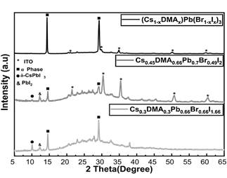
The relationships between the perovskite cations contribute to different properties of the final structure, where the lower the Cs content the higher the light absorption but lower stability of the α-cubic phase, while for lower DMA content an opposite behavior is observed. Therefore, it is necessary to find the harmony between the cations to obtain a pure phase, with good optoelectronic properties and acceptable stability. For this, different molar ratios such as 1:1:2, 1.36:0.74:2, and 0.3:0.7:0.7 were evaluated for a ratio between the composites DMAPbI3:PbBr2:CsI, producing the phases Cs0.3DMA0.3Pb0.66Br0.66I1.66, Cs0.45DMA0.66Pb0.7Br0.49I2, and (Cs1-xDMAx)Pb(Br1-xIx)3. It was found that the phases obtained using the composition Cs0.3DMA0.3Pb0.66Br0.66I1.66 and Cs0.45DMA0.66Pb0.7Br0.49I2 exhibited high phase mixing with less purity of the final structure, however, the (Cs1-xDMAx)Pb(Br1-xIx)3 phase is much purer with the appearance of characteristic peaks in XRD at 14.35° and 29.3° with high intensity, indicating a preferential orientation toward the desired α-phase (Fig. 4) [13]. Additionally, this phase exhibits a reduced background throughout the spectrum, indicating a lower concentration of amorphous phases.
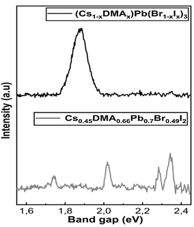
Moreover, in photoluminescence (PL) spectra, the composition producing phase mixture is found to have different emission peaks, indicating active phases with different band gaps. The band gap lower than 1.8 eV belongs to iodine-rich phases with low emissions, appearing around 10° in XRD, and the band gap higher than 2.2 eV to bromine-rich phases (Fig. 5), appearing in XRD between both characteristic peaks (between 14.35° and 29.3°)
Due to the purity of the (Cs1-xDMAx)Pb(Br1-xIx)3 phase, the upcoming experiments used this composition. Therefore, the spin coating deposition of the precursor was optimized to obtain films with different thicknesses (as shown in Table 1).
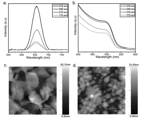
This is crucial because thicker films allow high light absorption which could improve the final device efficiency. To confirm this, optical characterization of these layers is performed, observing in the PL spectra an increase in the intensity of the emission peak at higher values of the layer thickness (Fig. 6a), as well as higher absorption in the UV-Vis spectrum (Fig. 6b). This means higher generation of charge carriers in perovskite films of higher thicknesses, producing a better optical behavior [14]. This is promising because perovskites with cations other than MA+ exhibit a lower absorption coefficient [15]. Therefore, enhancing charge carrier generation by increasing thickness inhibits the detrimental effect of replacing MA+ on radiation absorption.
To compare this perovskite with the most studied reference (MAPbI3), both perovskites were deposited and evaluated under the same conditions. Initially the AFM topography of both perovskites films was studied, in the case of the perovskite with reduced organic content the typical flake morphology of perovskites with high inorganic content was obtained (Fig. 6c) [13]. However, MAPbI3 perovskite presents spherical grains characteristic of MAPbI3 (Fig. 6d). For this type of materials, it is desirable to have grains as large as possible, providing higher electrical conductivity. In the case of flakes, the average size is about 450 nm. In contrast, the spherical grains size is around 150 nm, indicating a promising morphology of the perovskite under study.
To maintain the α-phase shown in XRD, it is desired to combine organic and inorganic cations in order to obtain a tolerance factor that yields pure cubic phase with geometric stability. For this purpose, the CsPbI3 perovskite was explored together with bromine and the organic perovskite DMAPbI3. The CsPbI3 structure has a very low tolerance factor leading to rapid decomposition under ambient conditions; on the other hand, DMAPbI3 is a structure with a tolerance factor higher than one and undesirable optoelectronic properties.
However, the combination of CsPbI3 and DMAPbI3 perovskites yield a structure with a tolerance factor in the ideal zone between 0.9 and 1, where the α-cubic phase necessary to maintain perovskite integrity for a longer time is produced. Combining these two cations increases the geometrical stability due to the size of the cations, which balances the structure and possibly the associated internal stresses. Li, Zhen et al. demonstrated that adding DMA to inorganic components such as cesium reduces the annealing temperature of perovskites, achieving the transition from the yellow δ phase to the black α phase at lower temperature [9]. This has also been evidenced in other reports suggesting that both the formation energy and the tolerance factor are favored by cation tuning leading to structural stability of the phase [11,16-18].
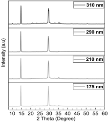
Now, analyzing the XRD of each of these conditions, it is found that there is a good reproducibility of the obtained phases (Fig. 7). However, the main peak at 14.35° indicates that the deposition conditions of higher spin coating velocity generate larger crystallite sizes, while lower velocities lead to thicker layers and smaller crystallite size (Table 2). This can be explained by changes in the evaporation rate during the process, leading to different nucleation points and crystallite growth rate. It is recommended in future works to continue the crystallization analysis to favor the increase in crystallite size at higher layer thickness, promoting the decrease in charge transfer resistance at the best thickness condition. This can be done with various additives that facilitate the increase in crystallite and grain size [19,20,21].
Source: own elaboration.
Figure 6 a. PL spectra of perovskite films at different thicknesses, b. UV-Vis spectra of perovskite films at different thicknesses, c. AFM image of perovskite (Cs1-xDMAx)Pb(Br1-xIx)3, AFM image of perovskite MAPbI3 (Scale 400 nm).
Table 2 Crystallite size at different deposition conditions
| Thickness (nm) | FWHM | Crystallite size (nm) |
|---|---|---|
| 310 | 0,226 | 35,339 |
| 290 | 0,228 | 35,125 |
| 210 | 0,214 | 37,401 |
| 175 | 0,193 | 41,509 |
Source: own elaboration.
Source: own elaboration.
Figure 7 XRD spectra of perovskite at different thicknesses Source: own elaboration.
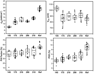
To correlate the variables studied here with the optoelectronic properties of the device, the solar cells described in the methodology section are made and compared with MAPbI3 as the reference perovskite (Fig. 8). We observed that on average the photovoltaic parameters closer to the reference correspond to the active layers with greater thickness, due to a better absorption of light. This is critical because this perovskite has a lower absorption coefficient than MAPbI3. Therefore, the thickness must be increased to provide a charge production comparable to that of MAPbI3.
Source: own elaboration.
Figure 8 Box charts of photovoltaic parameters of perovskite solar cells with different active layer thicknesses (nm).
Source: own elaboration.
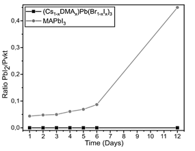
Figure 9 Comparative plot of the PbI2/Pvkt ratio in the perovskite (Cs1-xDMAx)Pb(Br1-xIx)3 and the reference. Study carried out at 30-40% relative humidity Source: own elaboration.
Finally, the stability of the (Cs1-xDMAx)Pb(Br1-xIx)3 perovskite was studied by comparing it with that of MAPbI3, where we observed that the time evolution of the PbI2 peak in the XRD spectra is significantly higher in MAPbI3 than in (Cs1-xDMAx)Pb(Br1-xIx)3 (Fig. 9). This indicates that the degradation rate at the conditions under study of MAPbI3 perovskite is higher than in (Cs1-xDMAx)Pb(Br1-xIx)3 perovskite. This figure shows that after 12 days, the MAPbI3 perovskite is considerably damaged by the returning to its main precursor, PbI2 however, the (Cs1-xDMAx)Pb(Br1-xIx)3 has not started to degrade yet.
4. Conclusions
Inorganic perovskites that minimize the organic component in their composition exhibit adequate properties and morphologies that address the fundamental stability issues of this class of semiconductors. In this study, we conclude that the most critical parameters to control are the layer thickness, morphology, and phase. This is due to the significant differences in optical properties, such as bandgap, and absorption coefficient, compared to conventional perovskites. Thus, finding appropriate parameters for depositing a high-purity layer that can be integrated into optoelectronic devices is crucial. Our results indicate that optimizing the process by adjusting molar ratios, perovskite concentration, and spin-coating parameters is necessary to control these variables.
Specifically, we developed an experimental procedure for depositing 300 nm (Cs1-xDMAx)Pb(Br1-xIx)3 perovskite layers that resulted in a pure phase material with the desired thickness and optical absorption properties. We used these layers to fabricate solar cells that achieved an average power conversion efficiency (PCE) of approximately 7.9%, which is equivalent to 80% of the PCE of the reference device.

