


 Inglés (pdf)
 Articulo en XML
 Referencias del artículo
 Enviar articulo por email
 Citado por SciELO
  Citado por Google
  Similares en
SciELO
Similares en
SciELO  Similares en Google
 Permalink
1. Introduction
The home electrical network of the city of Tunja obtains its energy mainly from processes of transformation of hydraulic and thermal energy into electric energy. These transformation processes affect the environment by producing polluting gases, the greenhouse effect in the case of thermal, or changing the climate of the region [1], that is why the use of photovoltaic panels presents a solution to reduce this environmental pollution.
Electric energy home consumption is not constant, it varies according to the days of the week, the months of the year, or specific circumstances that require it in each home, therefore, when implementing photovoltaic systems in home networks, the need of carrying out a study to estimate electricity consumption per hour increases, to be able to size systems that can reduce consumption peaks, and also reduce the costs in residential electrical assemblies.
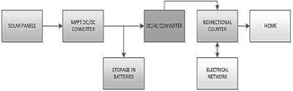
In this paper, a complete photovoltaic system is proposed, it takes energy from solar modules and through a DC-DC converter charges the battery obtaining the maximum possible power. Besides, it has a DC-AC converter as the final stage of the system, with specific characteristics that allow to comply with the two working modes: the first, called “constant average consumption system”, in which the consumption remains unchanged, pointing to the reduction in the variations that occur in a home for different reasons when the electric energy is used, but without reducing the total consumption; and the second mode is the “zero average consumption system”, where a total consumption of 0 Wh is desired.
In order to perform the connection to the network of the single-phase CSI topology, a series output inductance is required, which allows current control. In [2] the author presents a method to calculate the output filter CL with the aim to reduce the harmonic distortion, relating the switching frequency and the resonance frequency of the filter. According to the IEEE 519-1992 and IEEE 1547-2008 standards, power cannot be injected into the network with a 35th harmonic that exceeds 0.3% of the common connection point. Therefore, a network sensor is necessary to generate the waveform in phase and shape.
The system can supply energy to the electric network from two sources: the battery or the MPPT (Maximum Power Point Tracking) converter [3], and it must receive energy from the network if the solar modules are not capable of generating enough energy to charge the batteries [4] [5].
For this, the implementation of a bidirectional DC-AC converter is required, which, depending on the time of the day, it can deliver or take energy from the electrical network, and thus comply with the system specifications [6]. Without neglecting important analyzes regarding the photovoltaic system as a whole, this converter is the main object of study in the paper, that is why its design, model and implementation are presented in this work with their respective performance tests and conclusions.
2. System description
The proposed photovoltaic solar system has a positive impact on environmental pollution issues, and it also allows reducing variations in consumption to the home´s network, since it takes energy in hours of low consumption and delivers it in hours of maximum consumption.
In order to size the power of the system for home networks in the city of Tunja, energy consumption data was requested from the Boyacá Energy Company (EBSA), which made it easier for the previous work to this project, however, this information is confidential, therefore, the data set out below is not referenced.
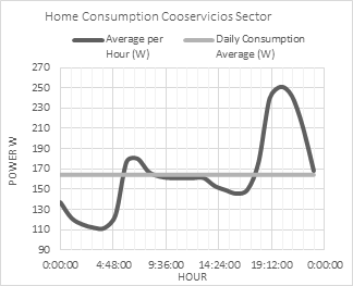
From the whole information about the energy consumption of the city of Tunja, the consumption data of the "Cooservicios" sector with a quantity of 8457 users was extracted. These data correspond to the average power consumed per hour from August 1, 2015 to August 4, 2016.
Fig. 1 shows the variations in average consumption per hour of a regular user in the sector, where the hours of greatest consumption are from 6:00 am to 9:00 am and from 6:00 pm to 10:00 p.m. The "Cooservicios" sector is mainly residential, so the consumption is below the daily average in the afternoon.
Source: The Authors.
Figure 1 Average consumption per hour of a home in the Cooservicios sector in the city of Tunja.
The power of the converter is determined from the data selected for the study, where it is found that the maximum average power per hour consumed by a home is 272 W. From the sizing of the solar field based on the data provided by the EBSA, it is known that the production of solar panels can have a peak of 400 W, so this power is chosen as the maximum value to design the converter, thus it can be adapted to a system without storage.
The battery bank voltage of the system is 72 V, and it represents the input of the converter to be designed, which can be a Voltage Source Inverter (VSI) or Current Source Inverter (CSI), however, as it requires an output of 120 Vrms a CSI (Current source inverter) inverter topology was chosen, unlike the VSI (Voltage source inverter), it is characterized by being a booster, so the boost converter at the output of the battery bank is omitted and the inverter is directly connected to the batteries.
Proposed solution
The proposed system to have an average consumption of electric energy equal to zero in a home of the city of Tunja, is the following system:
Fig. 2 shows the working mode, the batteries are charged with the energy obtained from the solar panels, and the system also delivers energy to the electrical network from the battery bank or the photovoltaic solar field directly. On the other hand, the system proposed with the aim to reduce the variations in electric energy consumption, Fig. 3 presenting a constant consumption in a home of the city of Tunja, is the following:
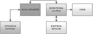
Now, in this second working mode, the system delivers energy from the battery bank to the electrical network. During the hours of maximum consumption, it reduces the losses on the grid, and the bank is only charged from the network in hours of lower consumption.
Taking into account the operation of each system, the CSI inverter to be implemented must have the ability to adapt itself to the characteristics of each case study: constant average system and zero average system.
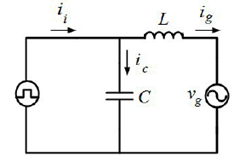
The CSI allows an input voltage lower than the peak of the electrical network; it has an input inductance and a CL filter at the output of the H-bridge, this is due to the fact that the converter must be connected to the electrical network, and as its output is in voltage, it is necessary to add an output inductance to ensure the injection of current into the network [8].
Besides, as it is known, the CSI is a boost-type converter that uses the inductance in series with the input voltage to produce a constant current source. It is important to point out that sinusoidal modulation is carried out in the H-bridge inverter, in order to generate an AC output with a low-frequency sinusoidal component that is filtered by the output capacitor [9].
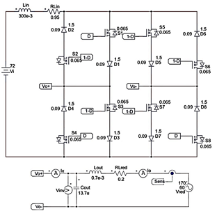
As the converter is able to deliver or take energy from the electrical network, the two cases are analyzed to find the correct switches, and the following topology shown in Fig. 4 is obtained:
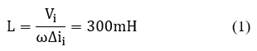
The input inductance of the converter can be calculated using eq. (1), in which, for an input voltage Vi of 72 V coming from the battery bank, assuming a ripple ∆ii of 10% and an efficiency of 80%, the inductance is:
The output filter is calculated taking into account that the input current is switched and filtered by the capacitor C (Fig. 5). In [2] the author presents a method to calculate this CL output filter to reduce the harmonic distortion, relating the switching frequency and the resonant frequency of the filter, obtaining a value of 13,7uF for the output capacitor C.
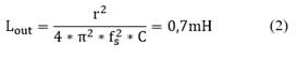
The grid connection inductance is calculated by eq. (2):
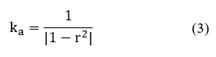
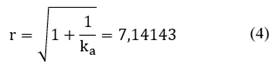
Where r is the ratio of the switching frequency to the resonant frequency of the filter, and it is related to an attenuation factor this way:
According to the IEEE 519-1992 and IEEE 1547-2008 standards, current cannot be injected into the network with harmonic 35 that exceeds 0,3% of the common connection point. The ka factor that satisfies the previous condition is 0,02 [2], obtaining a value of 7,14 (eq. (4)) for the variable r which is used to calculate the value of the output inductance in (2).
Modeling the circuit for each of its operating intervals, the expressions for the voltage in the input inductance, the current in the output capacitor and the voltage in the output inductance are obtained. Subsequently, applying the balance of volts per second and amps per second, the differential equations that govern the behavior of the circuit are also obtained, and the respective representation in state space is shown below in eq. (5):
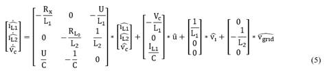
Where i L1 is the input inductance current, iL2 is the output inductance current, vc is the output capacitor voltage, vgrid is the converter input voltage, U is the control signal in a factor of 2D - 1 and Rx = RL1 + 2RD +2 Rdson where RD is the diode resistance and Rdson is the MOSFET on-resistance.
The transfer function for the state variable
 is shown in eq. (6):
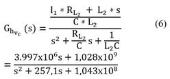
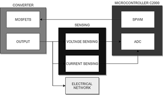
Fig. 6 shows a block diagram of the control signals of the switches were generated by means of the TMS 320F28377S microcontroller of the C2000 family of Texas Instruments, which has a frequency of 200MHz, flash memory of 1024KB, RAM of 164KB, 14 ADC channels of 12 bits and 16 High-resolution PWM channels. Below is shown a connection scheme between the microcontroller and the circuit:
Experimental results
The printed circuit of the power part of the converter was designed on a single board with 8 C3D16060D diodes, and 8 C3M0065090D MOSFETs with independent power supply or floating mode. The circuit was designed in a way that half of the area of the printed circuit board (PCB) is for the necessary components when the circuit is supplying power, and the other half when the system takes it from the electrical network.
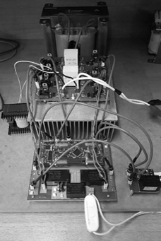
The final assembly of the circuit is seen in Fig. 7 and it is composed of the input inductance, the bidirectional converter, the microcontroller and the sensing board.
Source: The Authors.
Figure 6 Connection scheme between the converter, the microcontroller and the sensing system.
Source: The Authors.
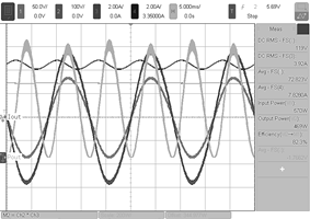
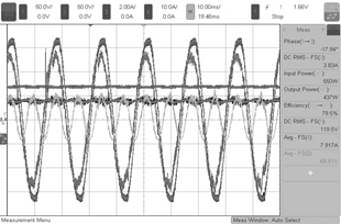
Figure 8 input voltage, output current, output voltage, input current, and output power.
The open-loop CSI converter was implemented with the output connected to a 30 Ω resistor that is capable of dissipating up to 4 kW. In the circuit implemented for this test, half of the arranged switches work. The test presented the following data.
Fig. 8 shows all the converter variables, there is a constant input voltage of 72,823 V and a current of 7,828 A on average, an output voltage of 119 Vrms and an output current of 3,92 Arms, for an efficiency of 82,3%. The power measurement was made on the input inductance and it was found that around 62 W are lost in it. Thanks to the power analysis tools of the Agilent MSO-X 4034A oscilloscope, the harmonic distortion of the current is calculated this way:
Fig. 9 shows a THD of 2,7% was obtained, and in a practical way a sweep in the modulation index is made to observe how the distortion varies with a constant output power. The following results are observed:
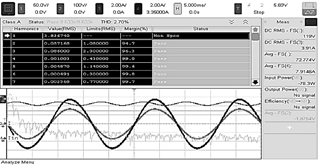
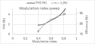
Table 1 and Fig. 10, shows how the harmonic distortion and the efficiency of the converter vary with variations in the modulation index:
It is observed that the harmonic distortion decreases if the modulation index is low, but the efficiency of the circuit also decreases. A relationship can be found between THD and efficiency in order to accomplish grid interconnection resistance of 30 Ω and an output voltage of 120 Vrms. The efficiency of the converter is 82,3% with an output power of 469 W and the power that is dissipated in the inductance is 60 W. Of the 100% of the circuit losses, approximately 60% is lost in the inductance, and the theoretical power loss over the switches is 46 W.
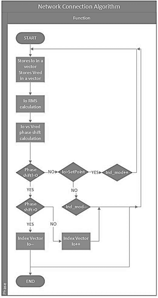
The connection of the converter to the network was made from the algorithm of the Fig. 11, which stores the voltage and current of the network in vectors to later find their RMS values, it also calculates the position where the zero of each function is located and thus to know how many positions the current must move to be in phase or counterphase with respect to the voltage, in case of delivering or receiving energy from the network, respectively.
4.1. Delivering energy to the electrical network (inverter mode)
In the Fig 12 is presented the data of the input and output current, network voltage and the power delivered to the network for the converter in inverter mode, that is, when it delivers energy to the electrical network:
It can be seen that 437 W are being delivered to the electrical network and the efficiency of the converter is 79,5%, the calculated harmonic distortion is 9,8% for the output current and 3,68% for the grid. There is a phase shift between the output current and the network voltage, this is due to the fact that the implemented algorithm presents variations in the operating point, this could be improved by storing more periods of the signals, although it would slow down the corrections against variations of the network in phase and in the current that is injected.
Table 1 Current source inverter design parameters, Ro=120 ohm.
| Modulation index | THD (%) | Po (W) | Io (Arms) | Vo (Vrms) | Vi (V) | Ii (A) | Pi (W) | ɳ (%) |
|---|---|---|---|---|---|---|---|---|
| 0,4 | 1,8 | 118 | 117,2 | 35,5 | 35,5 | 4,2 | 151 | 78,0 |
| 0,5 | 2,1 | 118 | 117,0 | 41,4 | 41,4 | 3,3 | 139 | 84,6 |
| 0,6 | 2,8 | 117 | 116,6 | 47,7 | 47,7 | 2,7 | 131 | 88,9 |
| 0,7 | 3,5 | 116 | 116,2 | 54,3 | 54,3 | 2,3 | 125 | 91,8 |
| 0,8 | 4,7 | 117 | 116,6 | 61,7 | 61,7 | 2,0 | 123 | 94,2 |
| 0,82 | 5,1 | 117 | 116,5 | 63,1 | 63,1 | 1,9 | 123 | 94,5 |
Source: The Authors
Source: The Authors.
Figure 12 electrical network voltage, electrical network current, input voltage, input current, and power delivered to the network.
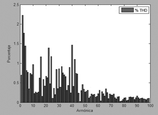
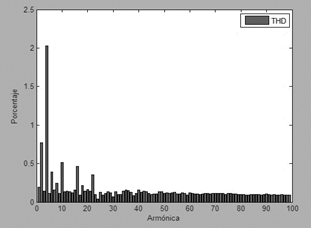
Fig. 13a shows the input current presents a component of 20% in the third harmonic, being the harmonic with the highest percentage, in the network voltage a fifth harmonic component is observed with 2% of the rms value of the network. Calculating the distortion in the current taking into account the current network distortion, it is found that the current has 7,82% THD respect to the network. When measuring the voltage of the electrical network, it is observed that it has harmonic content, this is observed in Fig 13b.
Conclusion
The operation of the converter has been verified in a bidirectional way, but with separate tests, an extra test is required to be able to program a consumption profile, and verify that the circuit is capable of generating a constant or zero average consumption per hour. Additionally, the implemented control presents variations in the operating point, this is due because an integral part addition is required.
The modulation index that determines the peak of the output current considering the input current, has influence in the THD and the efficiency of the circuit. When decreasing the modulation index, it affects positively the output signal by reducing its distortion, although at decreasing it, the efficiency of the circuit is also reduced, since it requires more current at the input.
In addition, from the transfer functions it is concluded that the input current does not affect the dynamics of the output current, because the input current does not vary regarding to the duty cycle.
The converter has a great disadvantage and it is given by the input inductance, since the value depends on the frequency of the electrical network and not on the switching frequency, making its value bigger, therefore, a large quantity of wire is required, which results in a large series resistance. This means, by having an inductance with a high series resistance and being a booster, the input current is greater than the output current and the losses in it will be squared every time the power increases.
Nevertheless, a comparison was made about the different configurations for the input inductance, and the configuration with a single inductance represents the best option, in price and in the value of the associated series resistance. In this sense, the circuit can be connected to a battery bank system and thanks to this input inductance, it can have a low current ripple without the need for an additional filter as it happens with the VSI inverter.

