


Services on Demand
Journal
Article
 text in
  Spanish (pdf)
 Article in xml format
 Article references
 Send this article by e-mail
Indicators
-
 Cited by SciELO
 -
 Access statistics
Related links
-
 Cited by Google
 -
 Similars in
SciELO
Similars in
SciELO -
 Similars in Google
Share

 Permalink
Ingeniería e Investigación
Print version ISSN 0120-5609
Ing. Investig. vol.31 no.1 Bogotá Jan./Apr. 2011
GaAs/AlGaAs nanoheterostructures: Simulation and application on high mobility transistors
Eduardo Martín Rodríguez.1, Estrella González R.2
1 M.Sc. in Electronic Systems Design, Universidad Tecnológica de la Habana, Cuba. eduardo.marin@electrica.cujae.edu.co
2 Electrical engineering. Ph.D. in Technical Sciences, Universidad Tecnológica de la Habana, Cuba. estrella@electrica.cujae.edu.co
ABSTRACT
This work analyses the features of GaAs/AlGaAs heterostructure, highlighting semiconductor junction properties. Charge confinement was produced when two materials having different band-gap were fixed; such high electron concentration is called two-dimensional electron gas (2DEG).
Device simulation for smart integrated systems (DESSIS) is simulation software which uses physical models and robust numerical methods for simulating semiconductor devices and 3-5 element heterostructures. Results for different heterostructure doping profiles and voltages are presented in this work.
High electron mobility transistors (HEMTs) are one of the most important applications for heterostructures; they work on 30 to 300 GHz frequency ranges. These transistors are simulated in this work; a 1 A/mm2 high current density was obtained in the channel, such value being comparable to other values reported for similar transistors.
Keywords: HEMT, heterostructure, DESSIS, simulation.
Received: October 9th 2009. Accepted: Feuary 7th 2011
Introduction
The word nanotechnology is widely used when talking about materials and different devices: electronic, photonic, magnetic, biological or molecular. However, it should be clarified that the term is valid when the core of the elements mentioned above have nanometer critical lengths, thereby making it possible to manipulate them with the same engineering precision (Beamont 1994). This should be born in mind when designing and constructing heterogeneous high integration and functionality nanosystems. Physical simulation of a device using powerful software is important during nanoscale device production cycle. Device simulation for smart integrated systems (DESSIS) has been used in this paper; it is a multidimensional simulation of semiconducting devices using advanced physical models and robust numerical methods.
DESSIS supports homostructured or heterostructured devices consisting of elements from periodic table groups 3-5. This software potential was used for simulating gallium arsenide (GaAs) and gallium aluminum arsenide (AlGaAs) heterostructure behavior and its application in high mobility transistors (HEMT).
HEMT, also known as heterostructure field effect transistors (HFET) or modulation-doped FET (MODFET) are a type of field effect transistor incorporating a conduction channel (rather than a doped region as in MOSFET), being a junction between two materials having different band-gaps. This is known as a heterojuntion.
The most used HEMTs are based on a combination of GaAs/AlGaAs, although there is a wide variety of them depending on the application in which are they going to be used (Chang 2006). Other HEMTs contain Indio; they generally have better performance at high frequencies (Martz 2005). Gallium nitride-based (GaN) transistors have been introduced recently, presenting better performance at high power (Mishra 2009). An example of applying the latter was recently presented by Fujitsu who developed a power amplifier based on the heterojunction of HEMTs made with GaN/AlGaN (Fujitsu 2010). These amplifiers provided transmission capacity 16 times higher than the equivalent with GaAs/AlGaAs.
Talk about integrated circuits using GaAs or 3-5 compounds began in the late 1970s (Notthoff and Zuleeg 1975). Silicon´s limits were beginning to be envisioned and this new technology began to find its place.
The first HEMT appeared on the market in 1985; it was invented by Minuro and Yokoyama from Japan. This was the transistor having the lowest noise at the time; it also led to work in the microwave range. These transistors found rapid applications in radio and terrestrial telecommunication systems (Fukuta 1999). One nanotechnology development line has focused on manufacturing compound semiconductor-based electronic devices (i.e. 3 -5 or 2-6 combinations) leading to small devices being made having low power consumption and transistors having high electronic density.
Applications working in the 30-300 GHz frequency range require active devices, such as high mobility transistors, called MMW HEMT (Milimiter-Wave HEMT). Antennas working on this wavelength must be smaller than 1mm and it is highly desirable that electronic modulation is immediately after the antenna, thus achieving very compact devices suitable for communication over short distances, for example in sensor network applications (Thayne 2004).
Considering MMW HEMT critical dimensions for a well-designed device, channel length determines the operating frequency (i.e. the smaller the faster the device). However, this is not enough; they must also have the least possible resistance and even the last Ohm has to be taken into account. Simulation plays a fundamental role in such designs.
The results presented in this paper are a first approach to nanoscale faication of high-mobility transistors using GaAs/AlGaAs heterostructure. The behaviour of energy bands for different situations is presented and the behaviour of current density in a channel for a high mobility transistor prototype is simulated and results are analysed and compared to those for other reports for similar devices.
Materials and Methods
Key features of GaAs / AlGaAs heterostructure
Using gallium arsenide (GaAs) to replace silicon as semiconductor material in active devices has been of great interest because electron mobility in GaAs is six times higher than that for silicon (8,600 cm2/Vs for GaAs and 1,350 cm2/Vs for Si).
Thus metal semiconductor field effect transistors MESFET) came to be faicated with GaAs, where electron mobility was higher than in silicon. MESFET circuits are faster than other types of silicon-based FET circuits and are known for their extraordinary speed (Rashid 2000). However, like other FET transistors, the GaAs semiconducting layer has to be doped to ensure electron mobility through it. These electrons slow down due to collisions with doping impurities. HEMTs resolve this problem.
HEMTs are FET transistors, the conduction channel being replaced by a junction where two semiconductor materials having different band gaps are joined. There is a very thin layer in which the Fermi level is above the conduction band. Carrier confinement is described as two-dimensional electron gas. Figure 1 gives a diagram of electron gas formation for a GaAs/AlGaAs heterostructure.
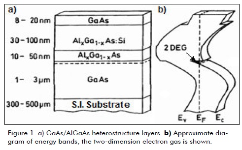
Figure 1a) shows that the layers forming the heterostructure begin with a semi-insulating substrate on which non-doped GaAs layer is deposited by epitaxial growth; it has a significantly lower band-gap than the AlGaAs-doped layers which follow. The different band-gap is why the electrons generated in the n-type AlGaAs thin layer all migrate to the GaAs layer left empty by the previous layer due to the heterojunction formed by the two materials having a different band-gap, forming a quantum well in the GaAs conduction band (Figure 1b). Here, electrons are able to move rapidly without hitting any impurities because this layer is non-doped and electrons are confined inside. The resultant effect is the formation of a very thin layer called two-dimension electron gas, having a great electron concentration and high carrier mobility, giving the channel very low resistivity. The x in the figure indicates the amount of Al present in the ternary compound. Increased x value in AlGaAs increases this compound´s band-gap, causing a growth in the number of electrons confined in the two-dimension electron gas.
The diagram shown in Figure 1b) is approximate because a correct diagram requires solving Poisson's equation, taking into account each layer´s doping and the resulting charge space.
In HEMTs, as in any FET transistor, gate voltage causes changes in conductivity in the two-dimension electron gas. The applied voltage between source and drain causes fast circulation for the electrons confined in the channel.
Due to the above conditions, charge carriers acquire very high mobility and high saturation speed, enabling them to react in the presence of very high frequency fields. The scattering effect produced on charge carriers by doping atoms becomes significantly reduced, meaning that the noise emitted by the device also becomes greatly reduced.
Normally, the two semiconductor materials have the same crystal structure for a suitable fit between them to prevent carriers being trapped in discontinuities that might occur, thereby lowering their performance (Cho 1994).
General DESSIS software features
DESSIS numerically simulates the electrical behaviour of a single semiconductor device or several physical devices combined in a circuit. Terminal currents [A], voltage [V] and charges [C] are computed on the basis of physical equations describing charge distribution and conduction mechanisms. A real semiconductor device, such as a transistor, is represented in the simulator as a virtual device whose physical properties are discretized in a grid or non-uniform mesh nodes.
Therefore, a virtual device is an approximation of a real device whose structure is described using the ISE TCAD tool by two files:
- A meshing or geometry file containing a description of the device regions, such as: boundary conditions, material types and locations of electrical outlets. This file also contains the location of all nodes and their connectivity; and
- A doping data file or device containing properties such as doping profiles and the way in which data is associated with discrete nodes.
DESSIS has many features. These can be summarised by the following:
- It contains a lot of models for physical devices and effects on semiconductor devices (thermodynamic and hydrodynamic diffusion models);
- General support for different geometries (1D, 2D and 3D);
- An extensive package for nonlinear solutions; and
- It allows interaction between electrothermal device models and circuit models designed in SPICE.
Main points about simulation using DESSIS
The geometry files and data mentioned above were generated using the tools in the MDRAW ISE TCAD package; such files were generated according to the geometry, doping profiles and loads which are applied to the system being studied.
DESSIS uses the main .cmd file which must be copied into the working directory (a .cmd file can be copied which has been used in other simulation and modified). The VI tool is used for editing the .cmd file which is a text-editing tool accessible from Linux operating system command line. The main file is divided by sections whose contents have to be reprogrammed according to the planned simulation. For example, the names of input files generated in MDRAW must be in the "Input files".
A .par file must then be created; it will contain all materials parameters in the design. This file is generated by typing: dessis-L <filename.cmd> in the command line. DESSIS thus creates the models.par file which has parameters for all materials in the structure.
Now, and due to their importance, mandatory changes in the .cmd file are described. For example, when working with ternary or quaternary materials, the molar fraction inside the physical section must be declared. The following were included in this simulation:
molefraction (xfraction=0.3
regionname=["region_1"]) # the region_1 represents the AlGaAs layer
As seen, it is very important to define the region where the ternary element is. The x value in the ternary element AlGaAs is treated as Al(x)Ga(1-x)As.
It has to be defined in the "solve" section that the Poisson equation is to be solved to obtain energy band distribution in the heterostructure:
solve{
Poisson coupled {Poisson electron hole}
}
The following commands must be defined in the "plot" section:
Plot {
hQuasiFermi
eQuasiFermi
EffectiveBandGap
ValenceBandEnergy
ConductionBandEnergy
}
Results and Discussion
Simulation of heterostructure and HEMT using DESSIS.
Simulating the energy bands in heterostructure is presented and their behaviour in different situations. The behaviour of current density in the channel of a high mobility transistor prototype is also simulated and results are analysed and compared with those for similar devices.
Band structure in the GaAs/AlGaAs heterostructure in different situations
Band structure behaviour was first simulated for the following heterostructure dimensions: GaAs (0.02μm) / AlGaAs (0.01μm) /GaAs (0.06μm). The result is shown in Figure 2.
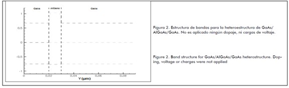
Doping profiles were not applied to the heterostructure in this simulation, nor were voltage loads applied to the system. A difference in GaAs and AlGaAs energy band gap may be noticed resulting from discontinuities forming in energy band structure at heterostructure interface.
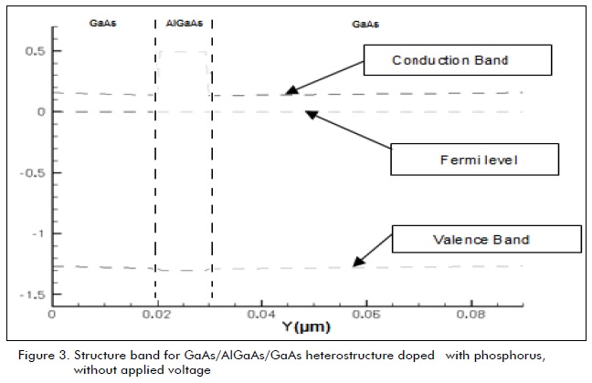
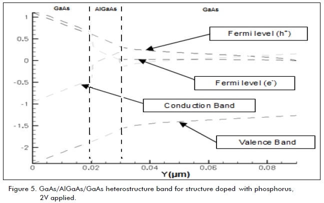
GaAs/AlGaAs heterostructure doped with phosphorus
Figure 3 shows the band diagram for a GaAs/AlGaAs heterostructure doped with phosphorus, making it possible to observe how the Fermi level approached the conduction band due to the doping effect with a donor element. Voltage source was not applied in this simulation.
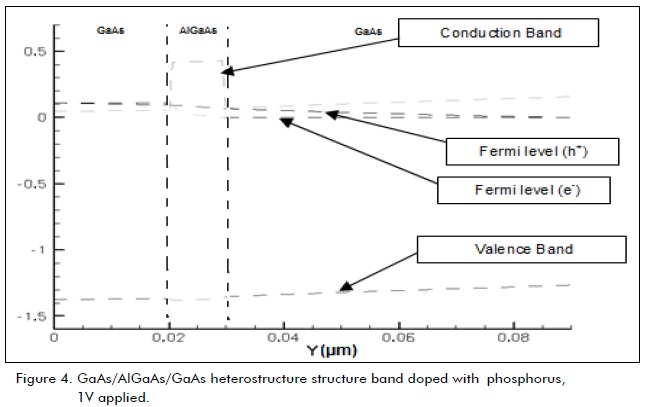
The following Figures show the behaviour of a phosphorusdoped structure when voltage was applied; in this case, behaviour for 1V and 2V can be seen. Figure 4(1V applied) shows a small tilt in valence and conduction bands, demonstrating the beginning of hole depletion.
Hole depletion is more evident in the following Figure (5) and high electron accumulation was reached. A very high negative charge current could be obtained in the heterostructure.
Current density pattern in the HEMT channel
AlGaAs/GaAs heterostructure can be used for faicating a GaAsbased field effect transistor (called HEMT as seen above), using a heterojunction from a thin AlGaAs layer having highly-doped n-type impurity and a thin undoped or slightly doped GaAs layer.
The electrons produced in the AlGaAs layer fell entirely to the GaAs layer and an electron beam was created in the material´s gap due to the difference, where electrons could move very quickly without colliding with any impurity. The main advantage of HEMTs on MESFETs was to create a conduction channel free of impurities caused by doping so that electrons could move freely. Such improvement reduced noise and allowed working at high frequencies and increased transistor gain. The following Figure shows the diagram for a DESSIS-simulated HEMT.
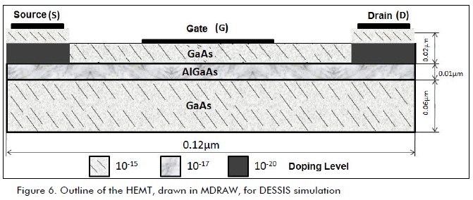
Two-dimensional electron gas formation in a GaAs slightly doped layer caused a large accumulation of electrons. This could also be modulated by the effect of gate voltage (VG). These transistors have a unipolar characteristic. The voltage applied between source and drain guided the electrons and allowed current conduction in the channel.
The simulation was performed for VSD = -1 V, VG = 1 V. The energy band diagram and current density pattern is shown in Figures 7 and 8.
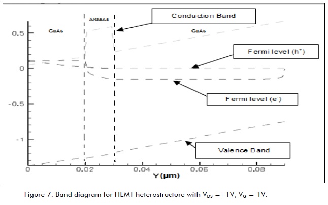
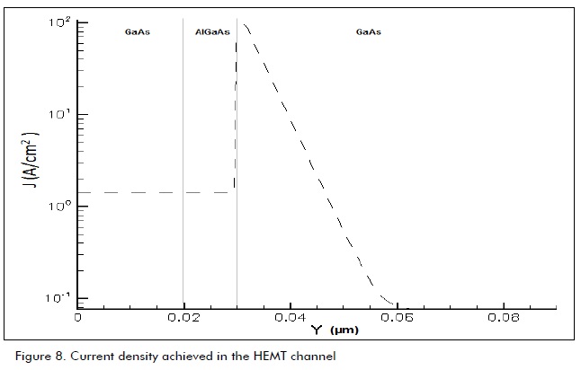
According to DESSIS, current density value was expressed in [A/cm 2] so that maximum current density in the HEMT channel was 1 A/mm2. Figure 8 shows that the maximum value for current density occurred at the place where the two-dimensional electron gas was, i.e. in the interface between the doped AlGaAs layer and the low doped GaAs layer.
An article setting out the results of a HEMT with 3-5 technology and 50 nm channel length (Thayne 2004), reported 0.9 A/mm2 current density for VDS = 1.2V and VG = 0V. These values were similar to those obtained in HEMT prototype simulation using DESSIS.
Conclusions
This work marks the beginning of simulating semiconductor nanostructures, which is undoubtedly a good result. Energy band patterns in the undoped heterostructure or that doped with phosphorous were obtained by simulation. The phosphorus doped structure pattern was also analysed by applying 1V and 2V voltages.
Current density values in HEMT were obtained from the simulation. The largest current value only occurred in the layer where the two-dimensional electron gas was. The values obtained were comparable with those reported by other authors. The good performance of a model implemented in DESSIS would thus seem to have been demonstrated.
This research focused on faicating small reliable and durable devices operating at high frequencies; these represent a key point these days for the scientific community. Achieving innovative and efficient designs are a big challenge, hence the importance of efficiently simulating these devices´ behaviour.
Referencias
Beamont, S. P., The applications of nanotechnology in electronic devices., IEEE Proceeding, 1994. [ Links ]
Chang, W. C., Improving breakdown voltage in AlGaAs/GaAs HEMT by gate oxidation., Journal of Optoelectronics and Advanced Materials, 8(1), 2006. [ Links ]
Martz, C., InP HEMT - Indium Phosphide High Electron Mobility Transistor., NASA Scientific and Technical Aerospace Reports, 43(15), 2005. [ Links ]
Mishra, U. K., AlGaN/GaN HEMTs: An overview of device operation and applications. Electrical & Computer Engineering Department., Santa Barbara, California, University of California. Ph.D., 2009. [ Links ]
Notthoff, J. K., Zuleeg, R., High speed, low power GaAs JFET [ Links ]
Cho, A. Y., Molecular Beam Epitaxy., AIP, 1994. [ Links ]
Fujitsu., Fujitsu develops GaN HEMT power amplifier featuring world's highest output in millimeter-wave W-Band., from http://www.physorg.com/news205606729.html, 2010. [ Links ]
Fukuta, M., History of HEMT Transistors., Journal of the JSPE, 1999. [ Links ]
Martz, C., InP HEMT - Indium Phosphide High Electron Mobility Transistor., NASA Scientific and Technical Aerospace Reports, 43(15), 2005. [ Links ]
Mishra, U. K., AlGaN/GaN HEMTs: An overview of device operation and applications. Electrical & Computer Engineering Department., Santa Barbara, California, University of California. Ph.D., 2009. [ Links ]
Notthoff, J. K., Zuleeg, R., High speed, low power GaAs JFET integrated circuits., IEDM Dig. Tech., Papers: 624, 1975. [ Links ]
Rashid, M. H., Circuitos microelectrónicos, análisis y diseño., University of Florida, 2000. [ Links ]
Thayne, I., Enabling nanofabrication., DTI Public Service Review, 2004. [ Links ]
Thayne, I., Very high performance 50nm T-gate III-V HEMTs enabled by Robust Nanofabrication Technologies., 4th IEEE Conference on Nanotechnology, 2004. [ Links ]

