


 English (pdf)
 Article in xml format
 Article references
 Send this article by e-mail
 Cited by SciELO
  Cited by Google
  Similars in
SciELO
Similars in
SciELO  Similars in Google
 Permalink
Introduction
Voltage followers or buffers are basic analog building blocks widely used as output stage in integrated circuits to drive low-level signals into loads owning large capacity. Thus, a good voltage follower should have: small input-capacitance together with high input-resistance as well as low-output resistance. Besides, it must be capable to deliver high output-current provided a low supply voltage, to preserve low-power consumption. Since designing an electronic circuit, where both large slew-rate and low-power consumption are demanded, conducts to contradictory constraints, traditional circuit techniques and topologies such as the well-known common-drain amplifier (Carusone, 2012) have been improved by means of innovative circuit techniques. Thus, during the past fifteen years, different circuit approaches have been proposed, such techniques range from the use of multiple-input floating-gate transistors (Ramirez-Angulo, 1995), Quasi-Floating-Gate (QFG) transistors (Ramirez-Angulo, 2003), and recently bulk-driven techniques (Haga, 2009). This last approach has become popular because it bases its low-power supply performance-capability in the reduction of the threshold voltage of P-MOS transistors by means of the body effect (Tsividis, 2010). However, it shows two main drawbacks when the bulk terminal is untied from the source: Lower input-resistance when the bulk is being used as signal input (Haga, 2009) and reduced signal dynamic range, since any the bulk-source or the bulk-drain junctions can be turned on, ending so, proper transistor function (Molinar-Solis, 2015).
The use of QFG transistors in MOS technology was introduced as an alternative to solve the "initial-charge" problem presented in true floating-gate transistors used for low-power implementations. Since then, it has been successfully used in analog applications ranging from baseband (Algueta-Miguel, 2011) to radio frequency (Xiang, 2012). The basic idea behind QFG circuits is to connect the transistor's gate to a bias point using a coupling capacitor and a very high resistance device (HiR). The key element is to use this capacitive coupling as a "floating battery" to control the AC response of the QFG transistor reducing the voltage supply requirements and consequently allowing low-voltage operation. In this work, the QFG concept is used to improve the flipped voltage follower (FVF) (Ramirez-Angulo, 2002) for achieving combined low-voltage and class AB operation.
This paper is organized as follows: In the next section, the proposed circuit is presented and explained. Section 3 presents some simulations of the proposed circuit using Spice and experimental results are discussed. Finally, in Section 4 conclusions are presented.
Quasi-floating Gate Flipped Voltage Follower
The proposed circuit is depicted in Figure 1. Transistors M1 to M3 form the basic structure of the FVF circuit, while M6 and HiR construct the biasing point for M5, which is in fact the QFG device. This transistor achieves class AB operation for this circuit in combination with M1; the circuit can be explained as follows: Considering large signal operation, the voltage swing at node "x" is coupled to gate of M5 through C1; if Vx rises, M5 is turned-off while vgsM1 is increased allowing M1 to sink large amounts of current from the output load. In contrast, if Vx falls, M1 is turned-off and M5 is turned "on", delivering more current to the output load (node "Vo"). For a proper operation of the circuit, it is required to M2 remain in saturation, then in DC Vx≈ VGSM1 +2V DSsa t +Vosw with VDSsat defined as the saturation drain-source voltage of a transistor, given by VDSsat ≥VGS -VTHN· Where VTHN is the threshold voltage of the NMOS transistor and the output swing is represented by Vosw Therefore, Vx must swing to control M1 and M5 but preserving M2 in saturation.
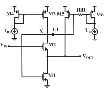
The capacitor C1 is a 2pF double poly-silicon parallel-plate structure and transistors sizes are depicted on Table I. There are several ways in CMOS technology to accomplish the required high value resistor (HiR) (Ramirez-Angulo, 2002). In this implementation, HiR was accomplished by two back to back connected diodes made by N-well and P+diff, as shown in Figure 2.
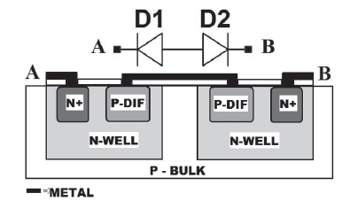
This diode structure was chosen because it presents a very low leakage current when is reverse-biased. Due to the lack of reliable diode models in the used technology, the diode voltage drop was characterized by measurements, resulting to be around 0,3V in 40 tested samples.
The small signal model of the FVF is depicted in Figure 3, where gmX = gml + gm5 and the bulk effect presented by the input transistor M2 is included by means of gmbM2. The output conductances of devices Mi are represented by goi. From this model, an approximated expression for the voltage gain (AV) of the proposed circuit was obtained by nodal analysis:
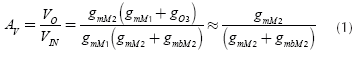
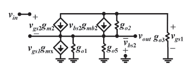
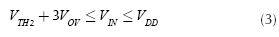
Equation (1) shows how go3 and gmbM2 deviates the voltage gain of this circuit from its ideal behavior. If the FVF is biased by an ideal current source having go3 = 0 and a technology with twin wells is available, where no bulk effect is exhibited by M2, Expression (1) turns to a unity voltage gain, which is desired by a voltage follower. However, since gmX >> go3, the last expression can be further simplified to the final form given. The aspect ratio of the involved transistors in (1), combined with their biasing currents, turn into a voltage gain of 0,77, which was later confirmed with measurements. Using this model, an approximated formula to estimate the output-resistance RO of the proposed circuit was found as follows:
Then, RO will be flat over the bandwidth of the circuit. For very high frequencies, where gmi decreases, RO will augment with frequency.
It is also of interest to find the range of voltages for which the cell is active. From Figure 1 and having into account the threshold voltage increment experienced by M2, (VTH2) and if all transistors are using the same over drive voltage (VOV), the following expression is found for the input voltage range (De Matteis, 2017):
Similarly, observation of Figure 1 shows: VGSM1=VX=2VOV, therefore, the output voltage range for proper operation of the circuit is bounded by (Molinar-Solis, 2015):
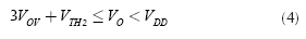
With VTH2 = 0,8V, VOV = 0,1V and VDD = 1,5V, both the maximum input and output signal swing would be around 0,4V.
Since the FVF is a second order system, stability is an important concern. Therefore, frequency behavior of the proposed circuit is analyzed by means of the high-frequency small-signal model given in Figure 4, where the main capacitances of the cell are given. Cgs and Cgd denote the gate- source and drain capacitances, respectively. CX is the capacitance connected directly from node X to ground, while CL is the total load capacitance connected to the output of the follower. CX is equal to:

CL is given by:
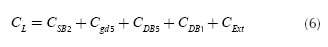
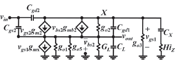
Where: CDB and CSB states for the drain-bulk and source-bulk junction capacitance respectively. CExt is any external capacitance connected to the output of the circuit, namely: pad, bonding wire, chip capsule, printed circuit board wire and measure equipment test-probes. GL is the total conductance connected at the output of the integrated circuit in a test bench, for instance, the conductance of the test-probes.
As it can be seen from Figure 4, HiZ and CX form a high-pass filter with cut-off frequency given by: 1/2ΠHiZCX. The output of this filter is connected to node "x", therefore, isolating biasing and signal of M5, being this cut-off frequency the minimum value for which the QFG technique has real effect over the circuit (Lopez-Martin, 2011).
Again, nodal analysis was used to obtain an expression for AV(s). Considering the most significant terms, as in Equation (1), the following simplified expression is obtained:
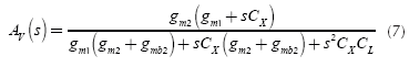
For DC, s = 0 Equation (7) reduces to Equation (1). As stated in Equation (7), the proposed circuit is a second order system with one zero and two complex poles. Although such a system is stable, a compensation network can be demanded to avoid excessive ringing in the transient step response of the circuit. In this work, compensation was added externally from node X to ground; in this way, CX is in parallel with the external compensation capacitor CC, therefore, the total capacitance at this point is: CT = CX + CC. From Equation (7), it is seen that a LHP zero located at -gmJ CX is present in the system. The effect of this zero can be cancelled with a nulling resistor (RZ) of value 1/gmX. As a good speed-accuracy trade-off, a damping factor ξ equal to 0,6 is usually chosen (Sekerkiran, 1997). Arranging the denominator of Equation (7) in the general form (Allen, 2002): s2 + 2ωLξs + ωL2, the following expression is found for ξ:
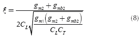
From Equation (8), solving for CT, and recalling that CT = CX + CC, it is produced:
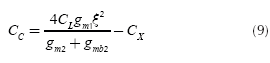
With ξ= 0,6, the compensation capacitor results in Cc≈ 12pF, while the nulling resistor RZ ≈ 1 kΩ.
Simulation and Measurement Results
The proposed feedback action over M1 and M5 is presented in Figure 5, which shows the simulated drain current. A transient analysis simulation was performed considering a 200mVpp square input voltage, Vin, and a DC bias of 1,3V at 2 MHz using LTSpice simulator (Linear, 2014). The complementary action of Id(M1) and Id(M5) is noticed in the plot, (Figure 5a), showing the source/sink current capability beyond the bias current.
The voltage at node "x" (Vx as shown in Fig. 5b), controls the sourcing/sinking current of M5 y M1 respectively with a capacitive load of CL = 18pF. As expected, the output Vo follows correctly the input Vin square signal. However, at node "x", both the drain of M2 and M3 are tied together, therefore is an inverting point with respect to the input-voltage. Consequently, as it can be observed in Figure 5a, as Vin goes down, Vx goes up, lowering VGSM5, thus, less current through M5 is available to be added to the current of M1 increasing the time needed to discharge the load capacitance. This is a direct result of the negative feedback present at this node, which tends to stabilize its voltage. The final effect is an asymmetry in Vo regarding rise- and fall- times of the cell.
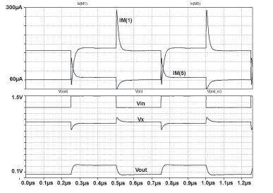
Source: Authors
Figure 5 Transient simulation with a 200mV square input signal; a) M1 and M5 drain currents (above); b) input/output voltages traces (below).
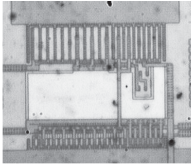
The microphotograph of the fabricated prototype is shown in Figure 6. The coupling capacitor C1 is at the middle of the circuit. The HiR structure lies left of the capacitor, which is in the middle of the cell. This block occupies a height of 92 μm and a width of 85 pm. The test chip was fabricated in a 0,5 μm, N-well, double poly CMOS technology available through The MOSIS Service.
To test the proposed cell, biasing currents Ib1 and Ib2 were fixed to 100 μA and 60 μA, respectively, by means of trimming resistors added externally to the chip. The used voltage supply was VDD = 1,5V. The values of the compensation network were adjusted to Rc = 1,2 k and
Cc = 10pF. Two biasing resistors forming a voltage divider were added to provide voltage bias to the input.
An experimental measurement of the test prototype is shown in Figure 7. The test was performed using a square signal Vin of 200mVpp@2MHz with a DC offset of 1,3 V added by the mentioned biasing resistor. The output follows the input voltage with a load CL = 22pF parallel connected to a resistor RL=10MΩ, this load is due to PCB parasites and oscilloscope probes. Test equipment characteristics are summarized in Table II
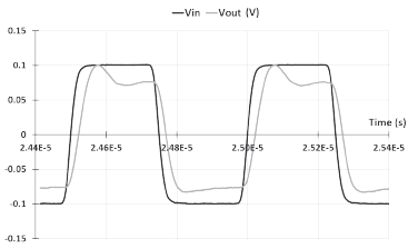
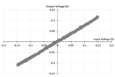
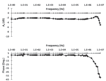
An oscilloscope plot of the low frequency transfer function of the circuit, Vin vs. Vo (mode X-Y), is shown in Figure 8. The slope of the trace suggests a voltage gain below one approximately 0,8, as suggested by Expression (1), this was later confirmed by an S-parameter measurement performed with a network analyzer; this plot shows a gain bandwidth product of 10 MHz (Figure 9).
Instrument Characteristics
In Figure 10, the linearity of the cell was characterized by means of the Fast Fourier Transform (FFT). After noticing the gain bandwidth product of the proposed follower, a test tone of 1MHz was introduced to the circuit, this frequency value was taken since it is where the test equipment has the best spectral purity. The output response of the circuit was traced in a digital-storage oscilloscope. This trace was captured at a sample rate (fS) fS = 12,5 MSamples per second in an external memory and thereafter processed off-line. The FFT was applied to the captured data. In the resulting power-spectral density trace, the main tone and its harmonics were identified with a simple algorithm (Jaeger, 2011) written in Octave (GNU Octave, 1993). After that, the total harmonic distortion (THD) was computed per the classic expression:
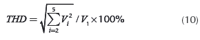
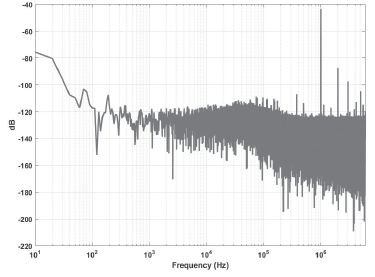
Due to the elected fS, only the first 5 harmonics (2...6 MHz) were included in the analysis, since the obtained spectrum is symmetrical at fS/2. The spectrum of the output signal from the chip is depicted in Figure 10. An experimental measurement of total harmonic distortion, THD = 1,12 % was obtained at 1 MHz, for an input amplitude of 140 mV.
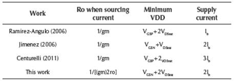
A comparison with other class-AB FVF's is presented in Table III. As can be noticed, the output resistance in this approach suggests an important improvement over other proposals when the circuit brings current to the output. The minimum voltage supply VDD and the power consumption is competitive to other approaches, therefore could be considered for low-voltage applications.
Conclusions
The design of a low-voltage class AB voltage follower was presented. In the proposed approach, class AB operation is accomplished by means of using a QFG MOS device connected in a negative feedback loop. A test prototype was fabricated in a CMOS 0,5mm double-poly process, where the threshold voltage of the devices is: VTHN = 0,7V and VTHP = -0,98V, for the N- and P- MOS transistors, respectively.
The test-cell was characterized and experimental results were presented bringing the following performance; a measured voltage gain AV = 0,77; gain bandwidth product of 10 MHz and a THD of 1,12 % @1 MHz. This building block occupies a silicon area of 92 pm x 85 μm and has a power consumption of 270 μW. An expression for the voltage gain of this circuit was presented, which is accurate with respect to the measured value.
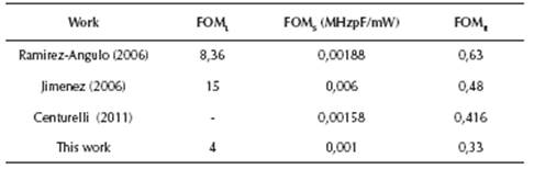
To conclude the present work, the figures of merit (FOM), proposed in Leung (2008), Peng (2004) and Leung (2000) are used to compare the proposed solution with other similar works: Ramirez-Angulo (2006), Jimenez (2006) and Centurelli (2011). The results are summarized in Table IV.
The large-signal FOML is dimensionless and defined as:
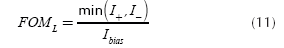
Where I+ is the positive-peak output current. I- the negative-peak output current and Ibias the total quiescent bias current. The small signal FOMS is given by:
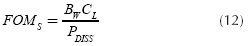
Where BW is the Bandwidth (MHz), CL the load capacitance (pF) and PDISS (mW) the total quiescent power dissipation. Finally, the signal-range Figure of Merit is dimensionless and defined by, FOMR:
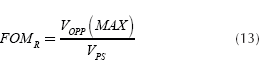
Here, VOPP(MAX) states for the maximum peak to peak voltage at the output and VPS is the power supply voltage.

