


 Inglês (pdf)
 Artigo em XML
 Referências do artigo
 Enviar este artigo por email
 Citado por SciELO
  Citado por Google
  Similares em
SciELO
Similares em
SciELO  Similares em Google
 Permalink
Introduction
One of the most characteristic features of today's scientific and technical progress is the extent to which electronic devices are used in many human activities, ranging from personal health to public safety, aerospace and defense. The elemental basis of such electronic devices consists of transistors, diodes, resistors, capacitors, and other elements designed and implemented in advanced micro- and later in nano-electronics. Based on recent scientific research, the economic analysis of market trends, and their contribution to social challenges, the European Union's (EU) Key Enabling Technologies (KET) include micro- and nano-electronics, nanotechnology, photonics, advanced materials, industrial biotechnology, and advanced manufacturing technologies (European Commission, 2012). These technologies are an engine of economic and technological development, as well as a major driver of innovation. In 2015, the global KET market was estimated at more than 1 trillion euros, while export of KET products from the EU accounted for up to 23% of exports worldwide. KETs also have great potential for growth and employment: in the coming years, 10-20% of growth potential can be expected (European Commission, 2013; European Commission, 2015). As a result, the European Commission, like other leading economy countries, has developed a strategy to boost the advancement of these high-impact technologies and create new workplaces, thereby boosting growth in other industries and sectors (European Commission, 2018).
At least 10% of the global GDP depends on products and services created by the micro- and nano-electronics industries (Annegarn, et al., 2012). These industries' innovations and their stimulating role is a major driver of growth in all electronics, information technology, automotive, aerospace, medical, and other economic industries. Therefore, the rapid growth of these sectors is also affecting the creation of new workplaces and the need for new employees, with a deeper knowledge. For example, according to the data of the statistical office of the EU (Eurostat), the number of Information and Communication Technology (ICT) professionals covering electronics, information technology, and telecommunications has increased by as much as 39,1% between 2011 and 2018, which is more than 6 times higher than the increase in overall employment of all sectors (6,5%). Similarly, more than two-thirds (63,1%) of ICT professionals in the EU had a university degree (Eurostat, 2018). The United States Bureau of Labor Statistics also projects the need for computer science and ICT professionals. According to forecasts, the employment opportunities of these specialists will increase by 12% between 2018 and 2028, i.e. much faster than the average for all other occupations. It is also forecasted that, during this period, about 0,55 million workplaces of this occupation will be created in the USA (United States Department of Labor, 2019).
Such rapid growth and development pose increasingly difficult challenges for higher education institutions. One of the major trials in a rapidly growing industry is to engage and motivate students to study engineering sciences. Most higher education institutions try to solve this problem by giving lectures and various seminars/workshops in secondary schools; organizing events, competitions, and tours with commercial enterprises; improving teacher competencies; and developing effective teaching methods and increasing their diversity. The second challenge, which we mentioned in our previous article and book (Barzdenas, Grazulevicius, and Vasjanov, 2020; Barzdenas, Navickas, 2012) is to provide quality education with minimal or no investment, as the costs of rapidly evolving technologies are very high. These costs, which include capital equipment, human resources, and time, are so expensive that higher education institutions cannot even make a dent with their limited financial resources. For these reasons, teachers are forced to look for virtual software tools that allow at least for the partial replacement of costly equipment. One such tool for virtual simulation of various micro- and nano-electronic structures and devices are various Technology Computer-Aided Design (TCAD) software tools. However, with the help of TCAD software tools, it is necessary to adopt various teaching methods to provide students with interesting tasks to motivate their better understanding of the common and newly developed structures of micro- and nano-electronic devices, as well as their working principles. Therefore, via laboratory projects and lectures, it is advisable to examine examples covering all stages of the manufacturing of these devices, that is, from an unprocessed silicon wafer to the simulation and analysis of the final structure of a semiconductor device and its electrical parameters and characteristics.
In this article, we describe the analysis of the processes used in micro- and nano-electronic device manufacturing. We also an example of a laboratory work where students use Silvaco TCAD software tools to apply a step-by-step approach to the design and simulation of an epitaxial planar n + pn transistor with junction isolation.
Design flow
Bipolar integrated circuits typically use n + pn transistors because their parameters are better than their pnp transistor counterparts. There are two reasons for this. First, the solubility of phosphorus, the impurity of choice for n-type materials, is higher in silicon than that of boron, which is conversely the dopant-of-choice for p-type materials. This leads to a higher impurity density in the emitter region and a higher emitter current transfer coefficient for n+pn transistors. Another reason is that the majority charge carrier of n + pn transistors are electrons whose mobility in silicon is several times higher than that of holes. This results in a higher current transfer coefficient. Additionally, with higher mobility, the transistors have better frequency characteristics and a higher operating speed. Therefore, in the presented laboratory work, we will simulate the manufacturing processes of n + pn bipolar transistors and show supporting Athena and Atlas software code with the explanation of its function.
The purpose of this laboratory work is to simulate the main manufacturing processes of an epitaxial planar n + pn transistor with junction isolation, as well as to extract the I-V characteristics of the obtained semiconductor structure. The main design stages of the technological process, described below, are as follows: silicon substrate preparation, formation of a n+ buried layer, silicon epitaxial layer growth, formation of junction isolation and collector region, formation of base region, formation of emitter and collector n+ regions, photolithography for contact windows, first aluminum metallization, passivation, description of transistor electrodes, analysis of transistor structure parameters, and simulation of I-V characteristics. All of these twelve stages performed in the laboratory work are shown in Figure 1.
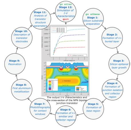
Source: Authors
Figure 1 n + pn bipolar junction transistor (BJT) step-by-step manufacturing and analysis flowchart.
Note: The authors would like to point out that the code below was generated and validated using Silvaco TCAD 2012 software for both Windows and Linux operating systems. It should also be noted that the word lifting symbol (-) in the code in this article means that these lines of code must be interpreted as a single line.
1. Silicon substrate preparation: The simulation of a planar epitaxy n + pn bipolar transistor and technological processes of other semiconductor structures with the Silvaco TCAD software can be performed by using the Athena software. This can be done by entering the following program code in the top of the Deckbuild program window:

Simulation of semiconductor structures and their technological processes begins with a description of the silicon wafer's dimensions. Since modern silicon wafers have a maximum diameter of 300 mm or 450 mm, and one transistor has the geometry of several or tens of micrometers, only the part of the wafer where the transistor structures will be formed is selected for simulation. The dimensions of the wafer are indicated along the axes of abscissas and ordinates. Our simulated transistor will have a starting point of the abscissa axis of 0 μm, an end point of 24 μm, and a start point of the ordinate axis of 0 μm and an end point of 4 μm. Later, the mesh (grid line) of the described wafer is formed. This is necessary because Athena uses the finite element method in its calculations. In this method, differential and integral equations are calculated at the intersection of the grid of abscissas and ordinates, so the denser the grid, the more accurate the calculations will be. However, it should be noted that grid density determines the calculation time, i.e. the denser it is, the longer the calculation time. Considering the accuracy of the simulation of the transistor structure and the calculation time, the following grid is chosen for further calculations: the abscissa axis will have a step grid of 0,5 μm at 0 pm and 24 μm point, and a denser step grid of 0,1 μm at 6 pm and 18 pm point, since μn junctions of the transistor will be created in this interval. Similarly, in the ordinate axis, a 0,1 μm grid is selected at the wafer's surface, and a 0,5 pm grid at the 4 μm point. The program code for the selected wafer and its grid description is as follows:

Subsequently, the wafer material and its crystallographic structure, doping impurities and their concentration, or the specific resistance p of the wafer are indicated. A silicon (Si) wafer with a (100) crystallographic structure, doped with boron and a specific resistance of p = 10Ωx cm, was chosen. The description code for such a silicon wafer is as follows:

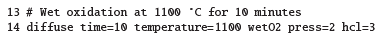
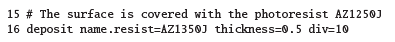
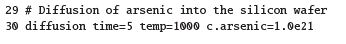
2. Formation of n+ buried layer: After preparing the surface of the Si wafer, a 10-minute thermal oxidation process is carried out in an atmosphere of wet oxygen at 1100 °C. The program code for thermal oxidation in wet oxygen is as follows:
We obtain 0,38 μm thick oxide, which is then coated with a photoresist in a centrifuge. Here, due to centrifugal forces, the photoresist spreads on a flat surface with a thin layer of 0,5 mm uniform thickness. The photoresist coating of the wafer with SiO2 layer is as follows:
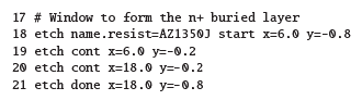
Thereafter, the technological process of photolithography should include the following processing operations: drying, exposing, heating, developing, and hardening of the photoresist. The photolithography process is replaced by the geometric etching used in Athena to simplify the program code. This etching removes the area of the photoresist specified by the coordinate points. The program code for geometric etching of the photoresist is as follows:
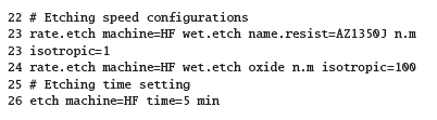
SiO2 is etched with fluoric acid HF using ammonium fluoride NH4F as an additive to improve the etching quality. The selectivity of such a mordant to the photoresist is very high (more than 100). The program code for isotropic etching is as follows:
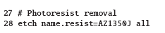
The remaining photoresist layer is removed in concentrated sulphuric or nitric acid. The removal of the photoresist is described below:
It is now possible to perform the initial formation of the n+ buried layer. At a depth of about 0,25 mm of the silicon wafer, a diffusion of arsenic (As) impurities at 1000 °C for 5 minutes is performed:
After this diffusion, the remaining SiO2 layer is etched using the following program code:
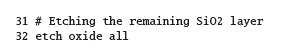
3. Silicon epitaxial layer growth: An epitaxial layer of 5 μm thick doped with n-type arsenic (ND = 5 x 1015 cm-3) is caused to grow on the wafer by using the chloride method in an epitaxial vertical reactor for 10 minutes at 1000 °C. The program code for this epitaxial process is as follows:
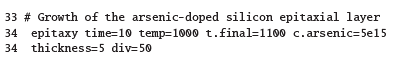
4. Formation of junction isolation and collector region: The wafer is thermally oxidized, and, during the second photolithography step, windows are etched in the areas where the two-stage boron diffusion will occur. The first diffusion is the doping of boron impurities at 1100 °Cfor 10 minutes, and the second diffusion is the redistribution of boron impurities at 1200 °C under a dry oxygen atmosphere. The duration of the second stage is chosen so that the boron impurities penetrate the entire thickness of the epitaxial layer. In this way, an n conductivity collector area is isolated by the p+ conductivity areas. The program code for this stage is as follows:
5. Formation of base region: Thermal oxide is grown with a thickness of about 0,38 mm. The third photolithography step is used to open the window of the base of the transistor in the oxide. Through this window, boron diffusion is also carried out in two stages. The target reference parameters of the base layer are: a depth XjB ofabout 1,5-2,0 mm, a sheet resistance RsB of about 250-300 Ω/□, and a surface concentration N0B of about 4-5 x 1018 cm-3. During the second stage of diffusion, the oxide layer that has grown in the base area is etched. The program code for this stage is as follows:
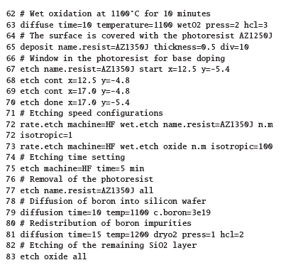
6. Formation of emitter and collector n+ regions: During the fourth photolithography step, windows for emitter diffusion and collector resistance reduction are formed. The n+ emitter is obtained through one-stage diffusion of phosphorus in an oxidizing medium for 5 minutes at 1000 °C. The target reference parameters of the emitter layerare as follows: the depth XjE is about 0,7-0,9 mm, the sheet resistance RsE is about 8-10 Ω/□, and the surface concentration N0E is about 1,5-2,0 x 1020 cm-3. The program code for this stage is described below:
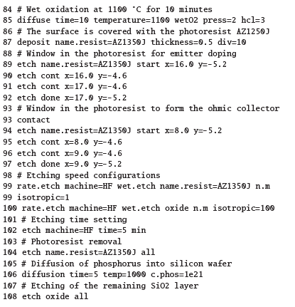
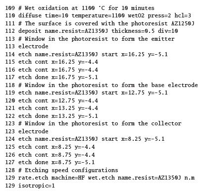
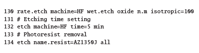
7. Photolithography for contact windows: The silicon wafer is thermally oxidized. The thickness of the oxide is about 0,38 mm. During the fifth photolithography step, windows are etched in areas where the transistor terminals, including the emitter, the base, the collector, and the junction isolation, create ohmic contacts between aluminum and silicon. After the oxide etching, the photoresist is removed. The program code for this stage is as follows:
8. First aluminum metallization: Before covering the aluminum layer through chemical vapor deposition, the wafer is cleaned by means of a chemical or plasma treatment. The projected Al layer thickness is 0,5 mm:
During the sixth photolithography step, windows for the transistor electrodes and other integrated circuit elements such as junction isolation are formed in the photoresist. The aluminum layer is then etched. Conductive paths, which are conductors connecting elements of integrated circuits, remain in the contact windows and on the insulating layer of silicon dioxide. The width of these conductive paths depends on the minimum size of photolithography and/or the maximum densities of the flowing current. Aluminum is etched in acid and alkaline solutions. In the case of a positive photoresist, Al is etched at 60-70 °C in phosphoric acid, and acetic, nitric acid additives are used to improve the etching quality. The etching speed of Al is about 550-600 nm/min, when the mordant solution contains 80% H3PO4, 5% HNO3, 5% CH3COOH, and 10% deionized H2O, and the temperature is 60 °C. Then, after removing the photoresist, annealing of the Al contacts is performed at 500 °C to improve the quality of the ohmic contacts. The program code for this stage is as follows:
9. Passivation: Finally, a continuous layer of silicon dioxide is deposited on the wafer's surface. Subsequently, the passivation photolithography step is performed to open windows for the final contacts/electrodes. These processes conclude the batch processing of transistors and integrated circuits with a single metallization on a silicon wafer. The program code is as follows:
10. Description of transistor electrodes: Once the transistor electrodes are formed, their names need to be specified to simulate the electrical characteristics of the created device. This is done by specifying the midpoints of the following electrodes in the abscissa axis:
11. Analysis of transistor structure parameters: During the manufacturing of the integrated device, the technological process must be monitored. The quality of oxidation, photolithography, and surface cleaning are visually checked. The parameters of the diffusion area are controlled by measuring sheet resistances Rs, impurity concentrations N0, and/or junction depths Xj. These parameters can also be fixed with Athena. The depths Xj of the resulting pn junctions at the middle of the emitter, i.e. the 16,5 abscissa point (x.val = 16,5) is found using the following program codes:

The junc.occno parameter specifies the order of the semiconductor layers from the substrate surface at the selected point (x.val = 16,5). Since, within the structure of the n + pn transistor, the emitter area is the first layer of the wafer's surface, then junc.occno = 1. Meanwhile, the base area is the second layer, and the collector is the third one, so these parameters are set to junc.occno = 2, junc.occno = 3, respectively.
After the calculations, the following results will be displayed in the bottom executable window of the Deckbuild:
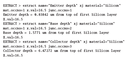
Calculations show that the emitter's depth (XjE) is approximately equal to 0,84 pm, the base XjB ≈ 1,58 pm, and the collector XjC ≈ 6,47 μm.
The sheet resistances Rs are determined using the following program codes:
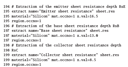
The calculations of the sheet resistance Rs give the following results: RsE ≈ 8,92 Ω/□, RsB ≈ 302,93 Ω/□, RsC ≈ 6,84 Ω/□.
The surface impurity concentrations N0 of the formed n + pn transistor areas are determined using the following program codes:
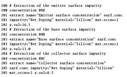
The calculations of the transistor areas N0 gives the following results: N0E ≈ 1,96 x 1020 cm-3, N0B ≈ 2,43 x 1018 cm-3, collector N0C = 1,82 x 1020 cm-3.
Finally, after fixing all the necessary parameters, the designed structure of the n + pn transistor with junction isolation is saved in the file completeBJT.str and represented by the TonyPlot:
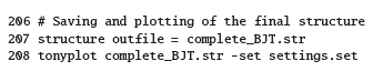
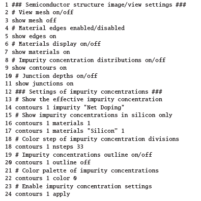
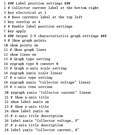
It should be noted that the TonyPlot has a specified text setting file (settings.set). This file stores the graph settings, text sizes, label names, etc. Therefore, when a Tonyplot graph is configured for the first time, this information is saved and reused as a template when creating new graphs and images. An example of this file is provided in Appendix A at the end of this article.
When all commands discussed above are saved in the Deck-build program window, calculations are performed. During this process, the TonyPlot will show the structure of a planar epitaxial bipolar n + pn transistor and the impurity distribution in the semiconductor volume. It can be seen in Figure 2.
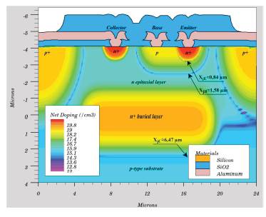
Previously, Xj setup program codes were provided, but this can also be done graphically. To do this, select the sequence of commands Plot → Display → Junction in the TonyPlot window, and when it is executed, pn junction boundaries will be plotted. To set these boundaries accurately, it is advisable to use a ruler that can be selected by executing the Tools → Ruler command sequence. After making measurements at the middle of the emitter, i.e. at 16,5 pm abscissa point, it can be seen that XjE → 0,84 pm, XjB → 1,58 pm, and XjC → 6,47 pm. The results of the measurements are presented in Figures 2 and 3.
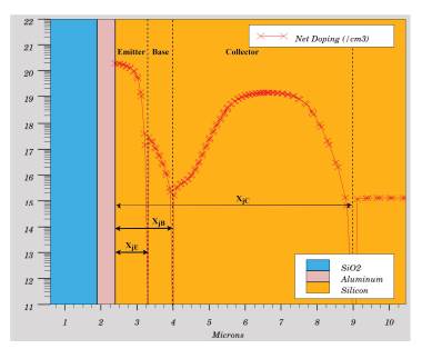
The Tools → Cutline command sequence is used to determine the impurity distribution in the desired areas of the semiconductor structure. After executing this command and selecting the vertical cursor, the desired point of the abscissa axis (in this case, the middle of the emitter, x = 16,5 μm) generates a graph of the net doping Neff (Figure 3). Neff is the modulus of the difference between donor ND and acceptor NA impurities, i.e. Neff = |ND-NA|. This graph can also be used to determine the Xj depths of pn junctions. Knowing that pn junctions are formed at a depth where the concentration of doped donor impurities is equal to the concentration of acceptor impurity (i.e. Neff = |ND-NA| = 0), the minima of this graph will correspond to the previously calculated and measured values of XjE, XjB, and XjC.
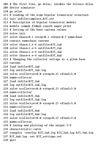
12. Simulation of I-V characteristics: Here is the program code for simulation of the output I-V characteristics family of a planar epitaxial bipolar n + pn transistor:
An example of the BJT_settings.set settings file is given in Appendix B.
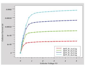
Figure 4 shows the family of the output I-V characteristics of a bipolar n + pn transistor. These characteristics show that the current of the collector IC is controlled by the current of the base IB. When VC = 2 V, and when the IB current changes from 1 μA to 2 μA, the collector current IC increases from 50 μA to 100 μA, that is, the base current transfer coefficient β is about 50.
Conclusions
The design and analysis of the manufacturing processes were performed for an epitaxial planar n + pn bipolar transistor with junction isolation, using only the seven photolithography steps. The basic design parameters of the transistor are given below. The crystallographic orientation of the silicon wafer is (100), doped with boron, and the specific resistance is p = 10 Ω x cm. The epitaxial layer of silicon is 5 pm thick, n-type, and has a surface concentration of ND = 5 x 1015 cm-3. The depth of the emitter is approximately equal to XjE ≈ 0,84 pm, the base XjB ≈ 1,58 pm, and the buried layer (collector) XjC ≈ 6,47 pm. Sheet resistance is, respectively, RsE = 8,92 Ω/□, RsB = 302,93 Ω/□ and RsC = 6,84 Q/D, and the surface concentrations N0E ≈ 1,96 x 1020 cm-3, N0B ≈ 2,43x1018 cm-3, and N0C = 1,82 x 1020 cm-3, respectively.
Discussions
At first glance, this kind of laboratory work may be considered 'dry', when merely entering the specified program code and realizing the supplied transistor structure without much further consideration. If students mechanically or monotonously enter the program code without delving into its meaning, syntax, and sequence, they do not acquire new knowledge, and, thus, the laboratory work becomes boring for them. To avoid this scenario, it is also necessary to present additional interesting tasks or control questions or tests that will allow students to understand the essence of this laboratory work and consolidate their knowledge. Therefore, each laboratory work session should be divided into separate stages that define the basic steps or groups of steps in the manufacturing of the micro- and nano-electronics device being developed. For example, the laboratory work presented in this article distinguishes 12 main stages: silicon substrate preparation, formation of a n+ buried layer, silicon epitaxial layer growth, formation of junction isolation and collector region, formation of base region, formation of emitter and collector n+ regions, photolithography for contact windows, first aluminum metallization, passivation, description of transistor electrodes, analysis of transistor structure parameters, and simulation of I-V characteristics. All these stages are shown in Figure 1. At each of these stages, the student is given additional tasks, which are presented in the form of a test. These tasks include both theoretical questions that examine the student's knowledge gained during the lectures and practical questions/tasks, which allows them to assess their skills and understanding. For example, in the silicon substrate preparation stage, students are asked test questions about the silicon monocrystalline ingot growth technologies, the slicing methods of the silicon ingot, the standard wafer diameters and thickness, the basic process steps for wafer preparation, and similar questions, which are discussed in detail during the lectures. Meanwhile, the practical questions ask a variety of questions related to the TCAD program code that were performed during laboratory work: how the dimensions of the silicon wafer are described, what the purpose of the mesh and its density is, among others. Practical questions also include asking students to create teacher-provided examples of silicon wafers with an appropriate or specific mesh. Meanwhile, in the final simulation of I-V characteristics, students answer theoretical questions related to the physical phenomena of BJTs, their regions of operation, different configurations for connecting BJTs, transistor testing methods, and so on. This article presents the program code for the output I-V characteristics family of BJTs. However, with a simple modification of this program code, the input I-V characteristics family can be obtained. Such modifications are given to students in practical tasks. From the obtained I-V characteristics, students can determine the basic parameters of BJTs: the common-emitter current transfer factor β, saturation and cut-off voltage points, transconductance, early voltage point, and others. The ability to simulate and analyze the I-V characteristics of transistors enables students to understand the theory of transistor operation, their basic parameters, and the technical specifications provided by manufacturers. This acquired knowledge and abilities allow students to properly use bipolar transistors to design various electronic devices.
After completing all these additional tasks, the student gets an assessment and proceeds to the next stage of this laboratory work. By completing all the stages and additional tasks, the student gets a final total grade.
Since these tasks do not require complex and expensive equipment, but only software tools, they can also be done remotely. In the case of most TCAD software packages, students can log in to their dedicated accounts or use licenses for these software tools remotely. Distance learning opens a wide range of opportunities for students and teachers alike. Students can learn and complete tasks with their own potential and at their own pace and time, and teachers, in turn, can come up with more interesting homework, course projects, or complex tasks that involve teams of students. This will enable students to further expand their knowledge and gain new research and experimentation experience while developing project management and people skills.
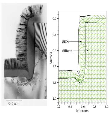
As mentioned earlier, teachers can also provide interesting course projects that students can do individually or in teams. For these projects, it is appropriate to give tasks from scientific publications that provide images or photos of real micro-and nano-electronic device structures. Students make an accurate computer simulation of these structures and analyze the obtained results by using the TCAD software tools and data from scientific publications. Two main advantages of such tasks could be highlighted. The first advantage is that students are convinced of the simulation accuracy of the TCAD software tools, and the second advantage is that students analyze scientific literature, which promotes scientific cognition and allows students to evaluate the possibilities of the practical application of scientific achievements. An example of one simple course project is shown in Figure 5.
Source: Authors
Figure 5 Oxidation in wet oxygen at 950 °C for 40 minutes: a) semiconductor structure photo (Marcus and Sheng, 1982); b) results of TCAD computer simulation.
This figure shows the growth specificity of silicon oxide, which depends on surface relief, various defects, and the formation of stresses. Students select appropriate materials and technological process parameters specified in the scientific article, and they simulate this structure and perform analysis with TCAD software tools. The results of this effort are submitted to the lecturer and presented to other students.
Valuable references which can be used as sources of theoretical material when coming up with tasks for students can be found in the referenced books and publications (Armstrong and Maiti, 2007; Maiti and Maiti, 2013; Maiti, 2017; Plummer, Deal, and Griffin, 2000; Sarkar, 2013).
This type of laboratory work, along with proposed tasks and control questions or tests, has been positively received by students at the Vilnius Gediminas Technical University. We have disclosed this in our previous article (Barzdenas, Grazulevicius, and Vasjanov, 2020) by providing capturing student feedback over several years. At the end of each laboratory work, a voluntary student survey is conducted to collect immediate feedback. Figure 6 and Table 1 show a subset of eight questions from this questionnaire. The answers of 83 fifth-year respondents were collected. For example, 81,93% and 85,54% of the respondents answered positively to the questions "Did you like carrying out this lab work?" and "Did this lab work provide you with new knowledge or skills?". Such a large number of positive responses indicates that students are both particularly receptive about the use of such laboratory work in the study process, and that it promotes the assimilation of the theoretical material introduced during lectures.


Conclusions
This paper presents an exemplary laboratory work cycle of manufacturing processes for micro- and nano-electronics devices. The aim of this laboratory work is to simulate the structure and I-V characteristics of an epitaxial planar n + pn bipolar transistor with junction isolation using Silvaco TCAD software tools. Seven photolithography steps were used to obtain the structure of this transistor: buried layer formation, junction transistor isolation and collector region formation, base region formation, emitter and collector n+ region formation, contact windows, first aluminum metallization, and passivation. This laboratory work also provides examples of the determination of sheet resistances, surface impurity concentrations, and junction depths of individual regions of the resulting bipolar transistor. Such laboratory work, which covers all device manufacturing processes and the simulation of their electrical characteristics, enables students to have a consistent view of the manufacturing process of such devices in order for them to deepen their knowledge gain new research and experimentation experience. In turn, this knowledge and these skills will enable students to contribute significantly in the future to the ever-growing development of micro- and nano-electronics and other industries and sectors.