


Services on Demand
Journal
Article
 English (pdf)
 Article in xml format
 Article references
 Send this article by e-mail
Indicators
-
 Cited by SciELO
 -
 Access statistics
Related links
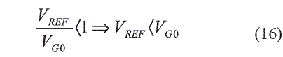
-
 Cited by Google
 -
 Similars in
SciELO
Similars in
SciELO -
 Similars in Google
Share

 Permalink
Revista Facultad de Ingeniería Universidad de Antioquia
Print version ISSN 0120-6230On-line version ISSN 2422-2844
Rev.fac.ing.univ. Antioquia no.60 Medellín Oct./Dec. 2011
Mathematical formulation of restrictions for the design of low voltage bandgap references
Formulación matemática de restricciones para el diseño de referencias de banda prohibida de bajo voltaje
Alicia Polanco*, Agnes Nagy, Manuel Álvarez
Microelectronics Research Center. Instituto Superior Politécnico José Antonio Echeverría. Habana, Cuba.
Abstract
Nowadays the qualities more looked for in the design of bandgap references are the low potential of the reference and the low value of its coefficient of temperature, being these parameters more favorable in curvature corrected bandgap references.
The design parameters of bandgap references depend on the value of the potential of reference VREF; nevertheless, in the reported designs there are not paid attention to conditions that limit the attainable value of VREF.
In this work the mathematical formulation of the restrictions that really limit the attainable value of the reference potential is presented in order that the design of a curvature corrected bandgap reference can be realizable.
Keywords: curvature correction, low temperature coefficient, low voltage bandgap references.
Resumen
Actualmente las cualidades más buscadas de las referencias bandgap son el bajo potencial de referencia y el bajo valor del coeficiente de temperatura, siendo estos parámetros más favorables en las referencias de bandgap con corrección de curvatura. Por otra parte y aunque claramente los parámetros de diseño dependen del valor del potencial de referencia VREF. Habitualmente en los diseños reportados no se analizan las condiciones que limitan el valor de VREF alcanzable.
En este trabajo se presenta la formulación matemática de las restricciones que realmente limitan el valor alcanzable del potencial de referencia para que el diseño de una fuente de referencia de bandgap con corrección de curvatura sea realizable.
Palabras clave:bajo coeficiente de temperatura, corrección de curvatura, referencia bandgap de bajo potencial.
Introduction
Bandgap voltage references are frequently used in analog circuits as voltage regulators and as such in A/D and D/A converters [1]. At present the qualities more looked for in the design of bandgap references are the low values of voltage and temperature coefficient [2,3].
Although the dependencies of design parameters on the wished value of reference voltage VREF are known, in the designs reported in the literature [3,4] the attainable value of VREF is rarely analyzed or its importance is neglected.
In this work the mathematical formulation of the restrictions that really limit the attainable VREF value and make a design of a curvature corrected bandgap reference realizable, are obtained. This value is verified experimentally through the design and measurement of bandgap type circuits, based on the sum of two base-emitter voltages.
Analysis of design equations
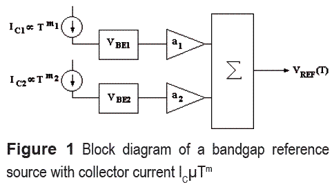
The block diagram of a low voltage bandgap reference, based on the sum of two base-emitter voltages is shown in figure 1 [2]. VBE1 and VBE2 stand for the expressions of the base-emitter voltages of the transistors and m1 and m2 determine the bias current temperature dependences [2,4,5].
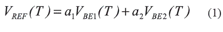
The expression of VREF (T) for the circuit of figure 1 is given by equation (1):
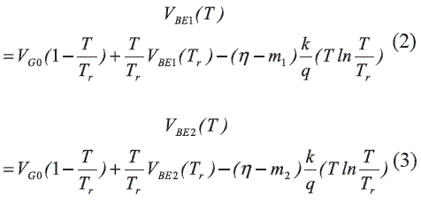
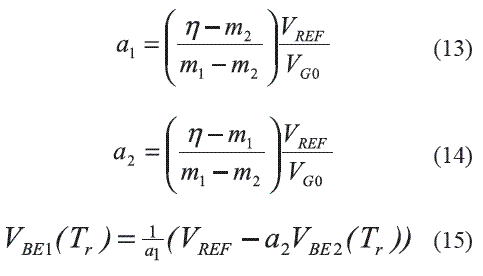
For the design of bandgap reference the parameters a1, a2, and VBE1 (Tr) of expression (1) should be determined, taking into account the known values m1 , m2 and VBE2 (Tr ).
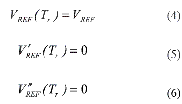
In order to reduce the temperature dependence of the reference voltage, that is VREF (T)=VREF the Taylor criterion will be applied.
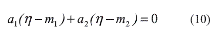
Using Taylor criterion at T= Tr, all possible derivates are zero around Tr, so the equations (4), (5) and (6) result:
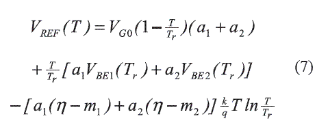
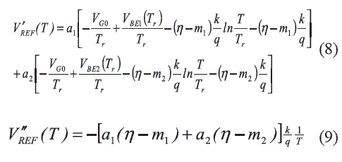
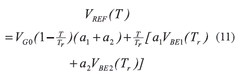
Considering (10) in (7), equation (11) results:
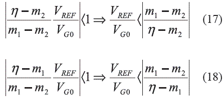
Analysis of the design restrictions
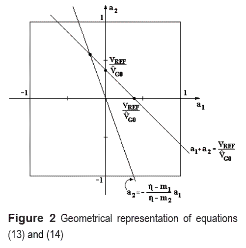
Equations (13) and (14) allow a convenient visualization of the design conditions when they are represented as lines in a1, a2 planes, as shown in figure 2 the solution for the design will be given by the intersection of both lines.
Use of the design restrictions in a practical case
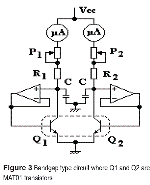
Criterion expressed in equations (16), (17) and (18)) was assessed experimentally through the design and measurements of the bandgap type circuit shown in figure 3, using constants (m1=0) and IPTAT (m2=1) bias currents.
A mathematical program was developed as a tool in order to:
Calculate the values of η and VGO for the transistors MAT01 used (based in experimental measurements of VBE at three different temperatures) and VREFMAX, for m1=0 and m2=1.
Calculate the design parameters a1, a2 and VBE1(Tr) for the wished VREF .
The requirements needed in the measurement of temperature, potential and current to obtain a mistake less than 0.25 ppm/ºC in the range 20 to 100 ºC were found by means of analysis of sensibility as:
a) Temperature: Resolution better than 0.01 ºC in the work range
b) Potential: Resolution better than 1 μV
c) The stability of the potentials VBE1(T) and VBE2(T) better than 0.2 μV respectively
For the measurement the following instruments were used:
- Astandard platinum resistor PT1000 DIN EN60751 as temperature sensor. The resistance of the PT1000 was measured with a Keithley digital electrometer model 614.
-Base-emitter voltages VBE1 (T) and VBE2 (T) were measured with the Keithley nanovoltmeter model 2182 with 100 nV resolution in a 1 V scale.
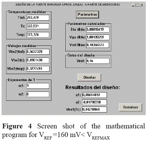
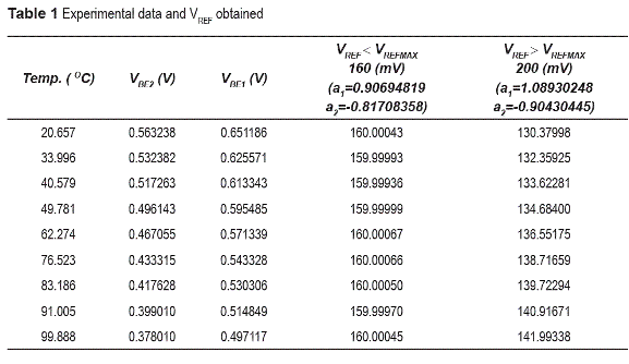
For the used MAT01 transistors the following values were obtained: η=588818419, VGO=1.08109259 V and VREFMAX=0.18360373 V.
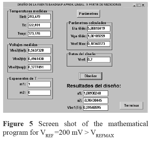
These results were used to calculate the design parameters in two cases (The screen shots of the mathematical program are shown in figure 4 and 5 respectively) :
a.) VREF=160 mV < VREFMAX (figure 4)
b.) VREF =200 mV > VREFMAX (figure 5)
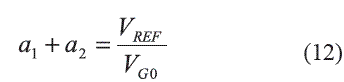
In screen shot of figure 5 the value of a1 > 1 can be observed. This value is out of [-1,1] interval (see figure 2) affecting the a2 value too in equation (12). , confirming that a design for VREF > 0.18360 V=VREFMAX is not possible.
The reference voltage were calculated in both cases, using in equation (1) the experimentally measured values of VBE1(T) and VBE2(T) together with the values a1 and a2 obtained by the mathematical program. The experimental measurements and calculated VREF values are shown in table 1.
In table 1 the values of VREF were obtained using equation (1). For VREF>VREFMAX case, VREF values result far away from the design one (200 mV) due to incorrect a1 and a2 values, showing that a target design value greater than VREFMAX is not attainable. Besides their increase with temperature invalids its use as a reference.
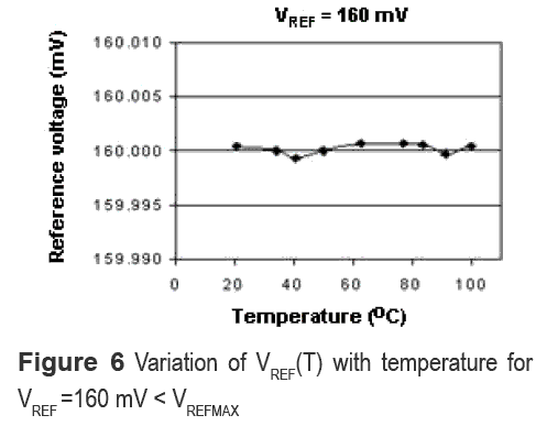
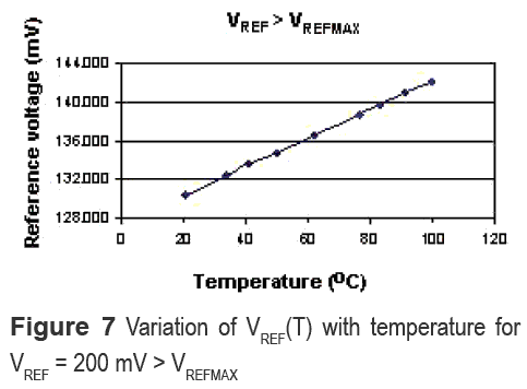
In figures 6 and 7 the variations of VREF with temperature are shown for both cases.
For VREF > VREFMAX case, VREF values result far away from the design one (200 mV) due to incorrect a1 and a2 values.
The reference voltage in figure 6, designed to 160 mV has an average temperature coefficient of U.1U1 ppm/ºC, while the one of the figure 7, designed to 200 mV shows an increase with temperature that invalids its use as a reference.
Conclusions
The analysis and the visualization of the design equations of a bandgap voltage reference based on the sum of two base-emitter voltages lead to obtain three equations that really limit the attainable value of the reference voltage VREF.
This means that VREF has to be less than the minor of the three quotas and can not overpass the value of VREFMAX.
This result was assessed experimentally through the design and measurement of a bandgap type circuit. The results show that the reference voltage designed to 160 mV < VREFMAX has an average temperature coefficient of 0.101 ppm/oC, while that designed to 200 mV > VREFMAX results far away from the design one, increasing with temperature. This behavior invalids its use as a reference. This fact confirms the importance of knowing restrictions that really limit the attainable value of reference voltages, aspect not studied up to now.
References
1. Analog Devices Inc. Data Converter Refernce Manual. Vol. 1. 1992. pp. 2-1141. [ Links ]
2. A. Van Staveren. Structures electronic design of high-performance low-voltage low-power references. PH.D. Thesis. Delft University of Technology. The Netherlands. 1997. pp. 155-180. [ Links ]
3. A. Pletersek. "A Compensated Bandgap Voltage Reference with Sub-1-V Supply Voltage". Analog Integrated Circuits and Signal Processing. Vol. 44. 2005. pp. 5-15. [ Links ]
4. G. C. M. Meijer, P. C Schmale, K. Van Zalinge. "A new curvature-corrected bandgap reference". IEEE Journal of Solid-State Circuits. Vol. 17. 1982. pp. 1139-1143. [ Links ]
5. C. Popa. "Optimal superior-order curvature-corrected voltage reference based on the weight difference of gate-source voltages". Analog Integrated Circuits and Signal Processing. Vol. 54. 2008. pp. 1-6. [ Links ]
6. A. Polanco, A. Nagy. M. Alvarez. "Physical design to verify theoretical 0.1 ppm/°C stability in a bandgap type circuit". Energía y Computación. Vol. 13. 2005. pp. 29-32. [ Links ]
7. R. Amador, A. Polanco, A. Nagy, M. Alvarez. "Accurate design of low-voltage curvature-corrected bandgap references". DCIS'2000. XV Design of Circuits and Integrated Systems Conferences. Le Corum. Montpellier. France. Nov. 21-24. 2000. [ Links ]
8. R. Amador, A. Polanco, A. Nagy. "The spread of η and VG0 and its influence on the sensitivity of a bipolar I.C Celsius sensor". Sensors and Actuators. Vol. 77. 1999. pp. 9-13. [ Links ]
(Recibido el 10 de agosto de 2009. Aceptado el 14 de abril de 2011)
*Autor de correspondencia: teléfono: + 53 + 07 + 645 29 35, correo electrónico: alicia.polanco@electrica.cujae.edu.cu. (A. Polanco)

