


Services on Demand
Journal
Article
 English (pdf)
 Article in xml format
 Article references
 Send this article by e-mail
Indicators
-
 Cited by SciELO
 -
 Access statistics
Related links
-
 Cited by Google
 -
 Similars in
SciELO
Similars in
SciELO -
 Similars in Google
Share

 Permalink
Revista Facultad de Ingeniería Universidad de Antioquia
Print version ISSN 0120-6230On-line version ISSN 2422-2844
Rev.fac.ing.univ. Antioquia no.60 Medellín Oct./Dec. 2011
A ripple-mitigating pre-amplifier based on interleaved DC-DC boost converters for efficiency improvement
Pre-Amplificador de potencia basado en conexión paralela de convertidores DC-DC para reducción de rizados de corriente e incremento de eficiencia
Eliana Arango1, Carlos Ramos-Paja*1, Carlos Carrejo2, Roberto Giral3, Andres Saavedra-Montes1
1Universidad Nacional de Colombia. Carrera 80 N.° 65-223. Medellín, Colombia.
2Laboratoire d'Analyse et d'Architecture des Systèmes LAAS-CNRS. Toulouse, France.
3Universitat Rovira i Virgili, Avda. Països Catalans 26, 43007. Tarragona, España.
Abstract
An efficient pre-amplifier based on interleaved DC-DC boost switching converters to mitigate high-frequency harmonics injection to power sources is proposed. The main features of the pre-amplifier are mitigate the ripple of power converters input-current and improving the efficiency of the whole power conversion chain. The pre-amplifier optimal operating conditions are calculated, and the circuit is modeled and controlled to operate in such conditions. The pre-amplifier interacting with a classical single boost is analyzed, obtaining a strong reduction in the current ripple injected to the source, and also improving the efficiency of the initial conversion system. Finally, the theoretical analyses are confirmed by means of circuital PSIM simulations and experimental results.
Keywords: Pre-Amplifier, interleaved converters, efficiency improvement, ripple mitigation.
Resumen
Este artículo propone un pre-amplificador basado en convertidores DC-DC conectados en paralelo para la reducción de armónicos inyectados a fuentes de potencia. Las principales características del pre-amplificador son la reducción del rizado de corriente de entrada en convertidores de potencia, incrementado además la eficiencia del sistema de conversión. Se describe el cálculo de las condiciones óptimas de operación del pre-amplificador, así como su modelado matemático y control para operar en las condiciones seleccionadas. Así mismo, se analiza el pre-amplificador con un convertidor elevador clásico, obteniendo una reducción significativa en el rizado de corriente inyectado a la fuente, así como un incremento en la eficiencia del sistema. Finalmente, los análisis teóricos se confirman a través de simulaciones circuitales y resultados experimentales.
Palabras clave:Pre-Amplificador, conexión en paralelo, eficiencia, reducción de rizado.
Introduction
Considering the problematic that establishes the global warming, fossil fuel exhaustion and the need to reduce carbon dioxide emissions provided the stimulus to develop renewable energies sources as fuel cell and photovoltaic panels [1, 2]. These options have been outlined for being two of the most attractive since they are clean, pollution free, and inexhaustible. An important aspect to consider is that these options have a series of disadvantages as the high costs of installation and maintenance, low diffusion among the users and difficulties in the process of energy storage, and such characteristics maintain them non-competitive opposite to the option of fossil-based energy resources. The appearance of new types of semiconductors, control strategies and switched devices has raised the relation cost benefit for this type of applications [3-6]. Nevertheless, the interconnection with the utility grid continues to be a weak point to consider.
It is widely known that the current harmonics generated in source-power converter interaction can seriously affect the system integrity and performance. In fuel cell applications, the current harmonics are directly related to the Oxygen- starvation phenomena, which considerably increase the natural aging of the cell membranes [7]. As for the photovoltaic applications, the current harmonics affect the performance of the control strategy, like the Maximum Power Point Tracking (MPPT) controller, reducing its accuracy and decreasing the system efficiency [8]. In this paper, the current harmonic injection to power sources by power converters is addressed through an active cancelation. Nevertheless, low frequency oscillations at double of the grid frequency are not considered since they can be addressed by control approaches [9].
This paper is based on the work "A Ripple- Mitigating Pre-filter Based on Interleaved DC- DC Boost Converters", developed by the authors, which appeared in the 36th Annual Conference of the IEEE Industrial Electronics Society (IECON-2010, © 2010 IEEE), and it is focused on the development of a power conversion system able to mitigate the high frequency current harmonics generated during the converter switching, which is traditionally addressed by the typical capacitor-filtering solution [10]. The proposed solution also reduces the input capacitor requirements, decreasing its cost and avoiding the use of non-reliable electrolytic capacitors.
The remain of the paper is organized as follows. The next section analyses a classical single boost converter considering power losses. Then, the novel pre-amplifier structure considering two boost converters in interleaved topology is introduced. Furthermore, the paper presents the proposed pre-amplifier operating with a boost converter, and compares it with the classical boost approach by analytical and PSIM simulation results. Moreover, the proposed solution is validated by means of experimental results. Finally, some conclusions of the work are given.
Single boost converter analysis
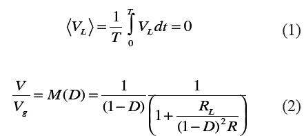
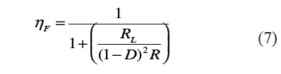
The design of a DC-DC converter, boost in this case, is performed to obtain the desired current and voltage ripples. Given the switching frequency, the input and output voltage, and ripples allowed, the capacitance and inductance are designed, which are largely responsible for the converter's size. The first step is to analyze the DC-DC boost converter efficiency considering the power losses lumped in a single inductor series-resistance as depicted in figure 1. Using the volt-second balance [11] (1), the relation between the input and output voltages (2) is obtained, where T is the switching period and D the steady-state duty cycle.
Pre-Amplifier topology and control
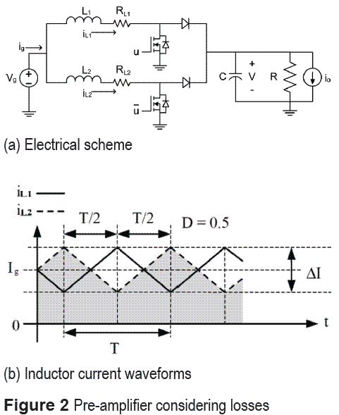
The pre-amplifier consists of two boost converters in parallel, analyzed by considering the power losses lumped in inductor series- resistances, which scheme is depicted in figure 2(a). The active switches, MOSFETs in this case, are controlled using complementary signals. This structure is called complementary interleaving and allows reducing the ripple of the input and output variables according to the specifications. The complementary activation of the switches in the boost converters cancels inductors current harmonics reducing the ripple in the input current [1].
Also, it mitigates the output voltage ripple and reduces the electromagnetic interferences. In this way, the reduction of the ripples allows to reduce the converter capacitances.
With the complementary control signals, one of the inductors current is increasing while the another one current is decreasing, therefore, the slopes of the current waveforms have opposite signs as depicted in figure 2(b), where T represents the switching period, D the duty cycle and ΔI the peak-to-peak ripple current. Since the input current is the sum of both inductor currents, the resulting slope tends to cero producing a decrease in the input current ripple. As shows figure 2(b), the most favorable ripple decreasing case is produced when the duty cycle is 0.5, or 50 %, because the slopes of both currents are equal but with opposite sign. The final value of the input current Ig corresponds to the integral of the shaded area.
Dynamic model
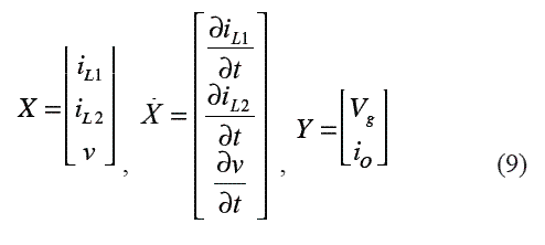
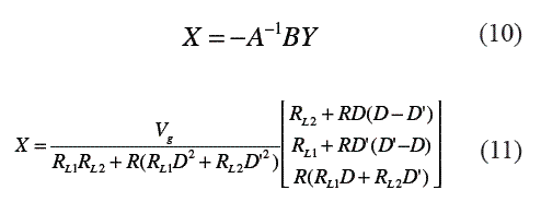
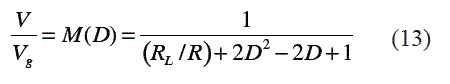
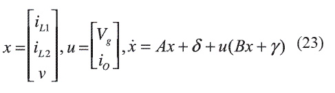
The state equations of the pre-amplifier circuit given in figure 2(a) can be expressed as:
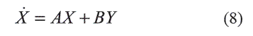
 correspond to the state variables vector and its derivatives. The Y vector contains the system inputs, and A and B matrices depend on the converter parameters.
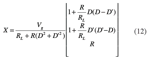

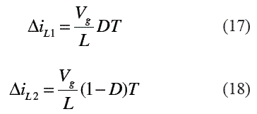
The current ripple magnitudes on the inductors are given by equations (17) and (18), obtained solving the charge balance (3) for each inductor in steady-state conditions:
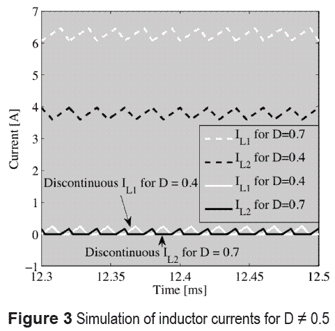
For D ≠ 0.5 one inductor enters on DCM because the CCM conditions given by (14) and (16) are not fulfilled. The inductor drove by the smaller duty cycle, and therefore with lower steady- state current, enters on DCM. This illustrated in figure 3, where a duty cycle D = 0.7 causes a discontinuous L2 current since it is driver by D', while D = 0.4 causes a discontinuous L1 current.
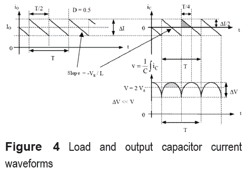
The output voltage ripple, depicted in figure 4, is calculated by analyzing the current waveforms of the load iO(t) and output capacitor iC(t). Figure 4 shows that the output voltage ripple is small enough to consider the load current to be constant and equal to its steady-state value. The current ripple is a sawtooth waveform with a frequency equal to the double of the switching frequency.
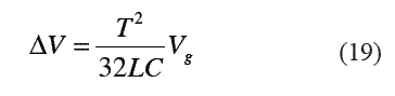
The voltage ripple is obtained by integrating the current ripple on the capacitor in each semi-period. It is observed in figure 4 that in each T/4 seconds the capacitor current sign changes, hence the capacitor voltage waveform is a symmetric convex parabola with a maximum value of (2Vg + ΔV/3). Calculating the integral of iC(t) through the triangular shaded area, the amplitude in absolute value of the output voltage ripple ΔV is calculated as:
Sliding-mode control
In practical implementations, there is slightly different impedances in both pre-amplifier branches, which causes a difference between the DC current components of the inductors depending on its inductance and parasitic losses tolerances. This must be addressed to ensure the ripple reduction, and therefore a closed loop control system is required. Since the PWM technique requires an external periodic signal, the sliding-mode technique has been adopted due to its simpler implementation.
The first step in sliding-mode control consists in the design of the state space region to which the dynamic of the system must be restricted, being generally called sliding surfaces. One option is to choose hyperplanes [2], meaning linear combinations of the system state variables.
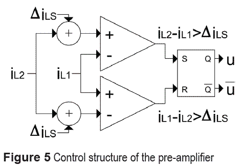
There are three state variables in the pre-amplifier. Two are the inductor currents and the last one is the voltage of the output capacitor. Although there are two switches, they are considered as a single control variable because they are activated by complementary signals, and therefore a single sliding surface S(x) is required to fulfill the desired condition D = 0.5:
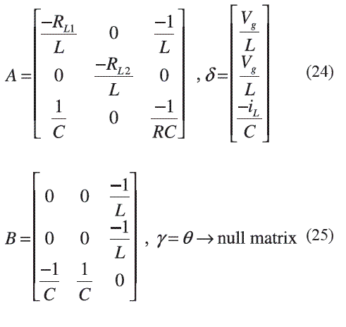
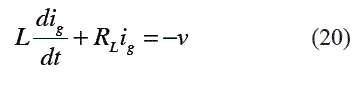
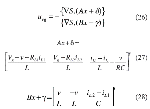
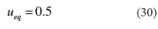
The equivalent control technique [2, 5] is used to calculate the continuous value ueq to be taken by the control variable (22) if the conditions S(x) = 0 and dS(x) / dt = 0 are achieved. Such conditions guarantee that the system trajectory is tangent to S(x) and remain trapped into it. The expression for the equivalent control is described by equation (26). In the numerator of the equivalent control there is the vector field (Ax + δ) whose expression, in this case, is given by equation (27), and likewise the denominator vector field is described by (28).
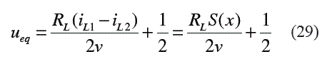
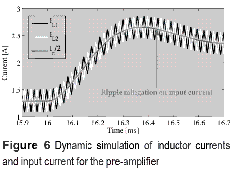
 are the complementary signals for activating the MOSFETs, and ΔiLs defines the maximum difference allowed between the inductor currents, therefore the width of the sliding surface. To illustrate the controller behavior, figure 6 shows a transient simulation where also in such conditions the inductor currents are complementary and the input current is minimum. In the simulation the input current is shown divided by two to allow its visualization in the same scale.
Pre-Amplifier based system: classicalboost interaction
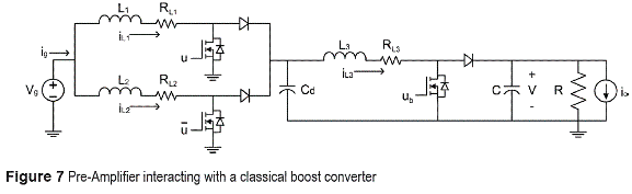
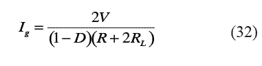
This section analyses the proposed Pre-Amplifier interacting with a classical boost converter as depicted in figura 7. The main objective of this structure is to reduce the current ripple injected to the source Vg without reducing the original power conversion efficiency. In this section, the input current ripple and the efficiency of both boost and boost with active pre-amplifier are contrasted.
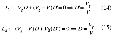
Steady-state analysis of the pre-amplifier based system
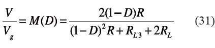
By applying the volt-second balance, and considering RL1 ≈ RL2 ≈ RL, the input-to-output voltage conversion ratio is:
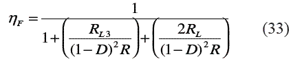
Comparison between pre-amplifier based solution and classical single boost
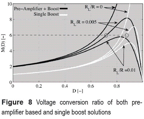
To perform a fair comparison, the power converters must be analyzed in the same conversion ratio condition and under the same load and source characteristics. The pre-amplifier based system has a higher voltage conversion ratio M(D) than the typical boost under the same source and load characteristics for a given duty cycle D. This is observed in figura 8, where considering a losses ratio RL/R = 0.005, or 0.5 %, a M(D) = 6 is obtained by operating the boost converter in the pre-amplifier based system at D = 0.72, while in single boost solution D = 0.88 is required. This is important since in boost converters the efficiency decrease with increments in D [11].
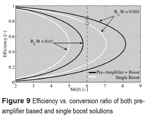
The pre-amplifier based system generates currents in each of the three inductors equal to the half of the inductor current in the single boost solution. Since the power losses depend on the square of the current, the losses in the pre-amplifier based solution are lower. This is depicted in figura 9, where considering M(D) = 6 and RL/R=0.005, the pre-amplifier based solution provides an efficiency of 0.83, or 83 %, while the single boost provides an efficiency of 0.76, or 76 %. Considering a different RL/R condition, the pre-amplifier solution also provides higher efficiency.
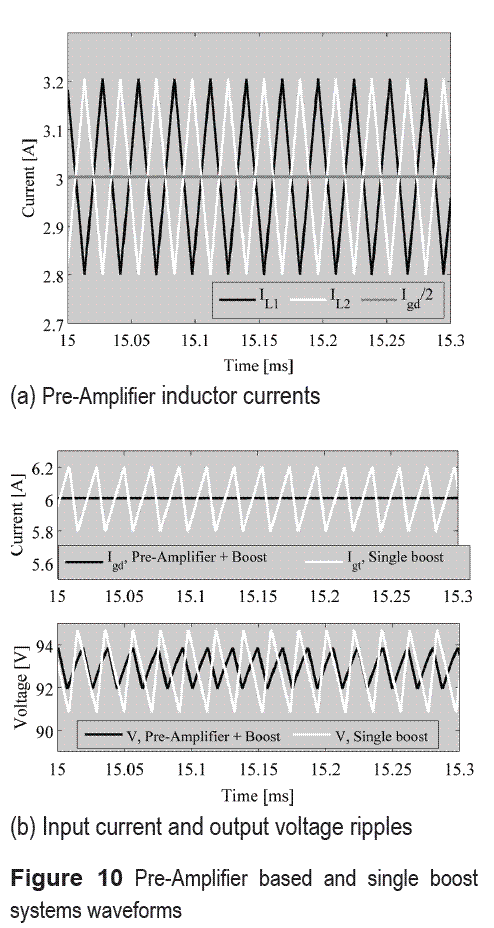
Figura 10 shows the simulation of the pre-amplifier based and single boost solutions. The waveforms of the pre-amplifier inductor currents and its input current, divided by two to allow its visualization in the same scale, are presented in figura 10(a). Such a simulation illustrates the complementary inductor current ripples, which interaction reduces the pre-amplifier input current ripple. The input current waveforms of the pre-amplifier based and single boost solutions are compared in the top of figura 10(b), which shows the significant reduction of the ripple injected to the source as described by (21).
Similarly, the reduction in the output voltage ripple in the pre-amplifier based solution, in comparison with the single boost solution, is depicted in the bottom of figura 10(b). Such an improvement is caused by the pre-amplifier voltage-boosting factor since in a boost converter the output voltage ripple depends on the difference between the input and output voltages.
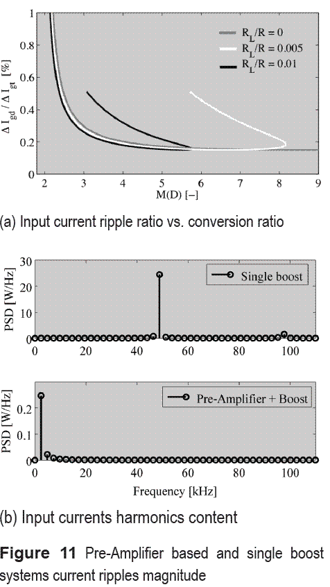
The input current ripple ratio {100 x ΔIgd/ΔIdt} [%] is defined to quantify the reduction on the current ripple achieved by the pre-amplifier based solution over the single boost converter.Figura 11(a) shows the input current ripple ratio depending on the voltage conversion ratio M(D) for different parasitic loss-resistance relations. It is observed that for M(D) > 3 the pre-amplifier strongly reduces the ripple injected to the source. In particular, considering M(D) = 6, the pre-amplifier based system generates only the 0.2 % of the single boost input current ripple.
Figura 11(b) shows the Power Spectral Density (PSD) of the input current harmonics for both pre-amplifier based and single boost solutions. It is observed a large harmonic component at the switching frequency in the single boost solution, while the PSD of the pre-amplifier based solution does not exhibit such a component due to the complementary inductor currents operation. In addition, the scale used to plot the PSD of the proposed solution is 100 times smaller than the one adopted for the single boost, which makes evident the strong harmonics reduction achieved.
Experimental results
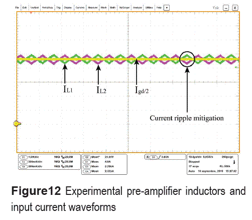
Experimental prototypes of the pre-amplifier based system, i.e. scheme of figura 7, and single boost solution, i.e. scheme of figura 1, have been developed to validate the analytical results. The inductors have been selected equal to 220 μH, the capacitors have been defined equal to 220 μF, obtaining a lumped parasitic resistances of 250 mΩ in each pre-amplifier branch and single boost converters. The load has been defined equal to 29.4 Ω, obtaining a parasitic losses ratio RL/R = 0.0085, or 0.85 %, which is comparable with the one defined in the circuital simulations. The inductor and capacitor values have been designed to achieve switching frequencies below 100 kHz and avoid electrolytic capacitors. The operating conditions have been defined by the input and output voltages Vg = 12 V and V = 40 V, respectively.
Figura 12 shows the experimental waveforms of the inductors and input currents of the pre-amplifier converter. It is observed the opposite inductor currents slope as well as the small ripple in the input current, which corresponds to a 1.3 % of the DC component. In contrast, for the same operating conditions, the single boost solution produces an input current ripple equal to 12 % of the requested DC component.
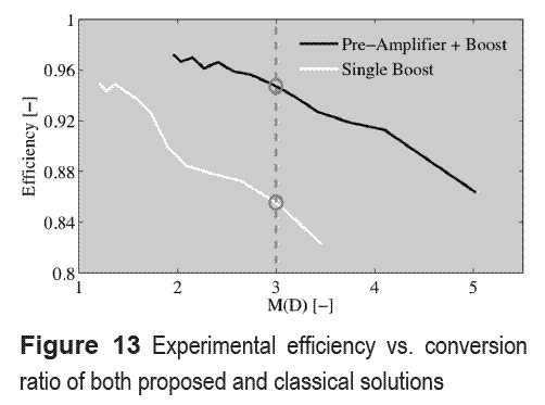
Figura 13 presents the experimental efficiencies of both pre-amplifier based and single boost solutions. The pre-amplifier based solution exhibits an efficiency improvement of 7.7 % over the single boost case at M(D) = 2, and the efficiency difference grows until M(D) = 3.5 up to 10.1 % where the losses in the single boost limits the voltage boosting ratio in such classical solution. Instead, the pre-amplifier based system is able to supply higher voltage boosting ratios up to M(D) = 5. Such experimental results, which have been carried out at an output power range between 16 W and 125 W, demonstrate the ripple mitigation and efficiency improvement provided by the proposed pre-amplifier based system.
Conclusions
This paper proposes a pre-amplifier aimed to reduce the current ripple injected to power sources by traditional DC/DC converters, being particularly analyzed with a boost converter. Besides, this solution improves the efficiency of the power conversion chain over the original system.
The proposed solution is based on interleaved boost converters, and it was analyzed in terms of efficiency and input current ripple. Its optimal operating conditions were calculated, and a sliding-mode controller was designed to ensure operation in such conditions.
The new power conversion chain, composed by the pre-amplifier and the original boost converter, was analyzed and contrasted with the original single boost solution. The theoretical analyses have been confirmed through PSIM circuital simulations, and experimental measurements validated the pre-amplifier benefits, obtaining a significant reduction up to 89 % of the original input current ripple, and an improvement on the efficiency between 7.7 % and 10.1 %.
Acknowledgments
This work was supported by GAUNAL and GITA research groups of the Universidad Nacional de Colombia (projects DACOGEN-PV and MECOVA-WIND), the Spanish Ministerio de Ciencia e Innovación (project TEC2009- 13172), and the Colombian Departamento Administrativo de Ciencia, Tecnología e Innovación COLCIENCIAS (scholarship 095-2005).
References
1. W. A. Surdoval, S. C. Singhal, G. L. McVay. The Solid State Energy Conversion Alliance SECA, U.S. Department of Energy Initiative to Promote the Development of Mass Customized Solid Oxide Fuel Cells for Low-Cost Power. The 7th International Symposium on Solid Oxide Fuel Cells. Tsukuba. 2001. pp. 1-10. [ Links ]
2. V. Acquaviva, P. Poggi, M. Muselli, Louche. "Grid- Connected Rooftop PV Systems for Reducing Voltage Drops at End". Energy. Vol. 25. 2000. pp. 741-756. [ Links ]
3. P. T. Krein, R. S. Balog, X. Geng. "High-frequency link inverter for fuel cells based on multiple-carrier pwm". IEEE Trans. Power Electron. Vol. 19. 2004. pp. 1279-1288. [ Links ]
4. C. Liu, A. Johnson, J. Lai. Modeling and control of a novel six-leg three-phase high power converter for low voltage fuel cell applications. IEEE Power Electron. Spec. Conf. Aachen. 2004. pp. 4715-4721. [ Links ]
5. C. Cabal, C. Alonso, A. Cid-Pastor, B. Estibals, L. Seguier, R. Leyva, G. Schweitz, J. Alzieu. Adaptive digital MPPT control for photovoltaic applications. IEEE International Symposium on Industrial Electronics. Vigo. 2007. pp. 2414-2419. [ Links ]
6. C. Cabal, A. Cid-Pastor, L. Seguier, B. Estibals, C. Alonso. Improved photovoltaic conversion chain with interleaved method. IEEE Power Electron. Spec. Conf. Island of Rhodes. 2008. pp. 70-75. [ Links ]
7. C. Haynes, W. J. Wepfer. "Characterizing heat transfer within a commercial-grade tubular solid oxide fuel cell for enhanced thermal management". Int. J. Hydrogen Energy. Vol. 26. pp. 369-379. [ Links ]
8. G. Grandi, D. Casadei, C. Rossi. "Direct coupling of power active filters with photovoltaic generation systems with improved MPPT capability". IEEE Power Tech Conf. Proceedings. Vol. 2. 2003. pp. 23-26. [ Links ]
9. E. Mamarelis, C. A. Ramos-Paja, G. Petrone, G. Spagnuolo, M. Vitelli. FPGA-based controller for mitigation of the 100 Hz oscillation in grid connected PV systems. IEEE International Conference on Industrial Technology ICIT. Viña del Mar. 2010. pp. 925-930. [ Links ]
10. S. J. Jang, C. Y. Won, B. K. Lee, J. Hur. "Fuel cell generation system with a new active clamping current- fed half-bridge converter". IEEE Trans. Energy Conversion. Vol. 22. 2007. pp. 332-340. [ Links ]
11. W. Erickson, D. Maksimovic. Fundamentals of Power Electronics. 2nd ed. Ed. Kluwer Academic Publishers. New York. 2001. pp. 39-77. [ Links ]
12. R. Girai, L. Martinez-Salamero, R. Leyva, J. Maixe. "Sliding-mode control of interleaved boost converters". IEEE Trans. on Circuits and Systems I. Vol. 47. 2000. pp.1330-1339 [ Links ]
(Recibido el 9 de diciembre de 2010. Aceptado el 20 de junio de 2011)
*Autor de correspondencia: teléfono: + 57 + 4 + 425 53 45, fax: +57 + 4+ 234 10 02, correo electrónico: caramosp@unal.edu.co (C. Ramos)

