


Services on Demand
Journal
Article
 English (pdf)
 Article in xml format
 Article references
 Send this article by e-mail
Indicators
-
 Cited by SciELO
 -
 Access statistics
Related links
-
 Cited by Google
 -
 Similars in
SciELO
Similars in
SciELO -
 Similars in Google
Share

 Permalink
Revista Facultad de Ingeniería Universidad de Antioquia
Print version ISSN 0120-6230
Rev.fac.ing.univ. Antioquia no.68 Medellín July/Sept. 2013
ARTÍCULO ORIGINAL
Reducing the hardware requirements in FPGA- based controllers: a photovoltaic application
Reducción de los requerimientos de hardware en controladores basados en FPGA: una aplicación fotovoltaica
E. Mamarelis1, C.A. Ramos-Paja2*, G. Petrone1, G. Spagnuolo1, M. Vitelli3, R. Giral4
1University of Salerno, D.I.E.M., Via Ponte Don Melillo 84084. Fisciano - Salerno - Italy.
2Universidad Nacional de Colombia, D.E.E.A, Carrera 80 No 65-223. Medellin - Colombia.
3Second University of Naples, D.I.I.I, Viale Beneduce N. 10, 81100. Caserta - Italy.
3Universitat Rovira i Virgili, D.E.E.E.A, Av. Paisos Catalans 26, Tarragona - Spain.
*Autor de correspondencia: teléfono: + 57 + 4 + 425 53 45, fax: + 57 + 4 + 234 10 02, correo electrónico: caramosp@unal.edu.co (C. Ramos)
(Recibido el 11 de julio de 2012. Aceptado el 19 de julio de 2013)
Abstract
Single-phase grid connected photovoltaic systems suffer from voltage oscillations due to the difference between the average power produced by the source and the pulsating instantaneous power injected into the grid. Such voltage variations have a detrimental effect on the power production. This paper proposes a solution for mitigating the oscillations at the source terminals minimizing the hardware resources required to implement the technique in a FPGA device, allowing its coexistence with additional control algorithms in a single device. The effectiveness of the approach was experimentally validated, and its FPGA resources requirement was contrasted with commercial IP cores based solutions.
Keywords: Photovoltaic, grid connection, FPGA implementation, resources requirement
Resumen
Sistemas fotovoltaicos monofásicos experimentan oscilaciones de voltaje debido a la diferencia entre la potencia promedio generada y la potencia instantánea inyectada a la red. Estas oscilaciones de voltaje degradan la producción de potencia. Este artículo propone una solución para mitigar las oscilaciones propagadas a las terminales del generador, la cual minimiza los recursos de hardware requeridos para implementar la técnica de compensación de un dispositivo FPGA, permitiendo su coexistencia con algoritmos de control adicionales en un solo dispositivo. La efectividad de la solución se valida experimentalmente, y sus requerimientos de hardware se contrastan con soluciones basadas en plataformas comerciales.
Palabras clave: Sistemas fotovoltaicos, conexión a la red, Implementación en FPGA, requerimiento de recursos
Introduction
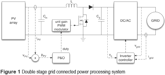
The typical Photovoltaic (PV) and fuel cell power processing system used for grid connected applications is composed of two stages, a dc/dc one and a dc/ac converter, connected through a dc-link, whose voltage is stabilized by a capacitor (Cb in Figure 1) [1]. In single phase applications, but also in three phases ones in which the equilibrium between the three-line currents is not perfectly preserved, the inverter operation generates an oscillation of the voltage across the bulk capacitor Cb at a frequency equal to the double of the line frequency and with an amplitude that is inversely dependent on the value of Cb [2]. This effect is mainly because the PV system generates a dc power and the inverter injects a pulsating power, at twice the line voltage frequency, into the grid. The bulk capacitor voltage oscillation back-propagates through the dc/dc converter and affects the PV voltage, thus degrading the Maximum Power Point Tracking (MPPT) performances and the global efficiency of the system [3]. In fuel cell systems, the oscillations reduce the stack lifetime [4] and degrade the available output power [5]. Traditionally, these drawbacks have been faced by choosing an enough high value of the DC-link capacitance Cb, but this results in a possible reduction of the system reliability because the employment of an electrolytic capacitor becomes mandatory [3], this technology being the only one ensuring high capacitance values. On the other hand, the adoption of non-electrolytic capacitors would lead to an expensive implementation, whenever a high capacitance value operating at a high voltage is needed [6].
Some papers, dedicated to both PV and fuel cell systems, propose different topologies aimed at reducing, or even at removing, the capacitance of the DC link. The price to pay is given by a lower efficiency or by an increased complexity in terms of layout and control techniques and, consequently, with additional costs [7, 8].
A different approach is adopted in some papers, in which the voltage oscillations affecting Cb in Figure 1 are filtered through a proper control strategy applied to the dc/dc converter. Such an approach avoids the drawbacks of the passive filtering, especially in terms of efficiency of the conversion chain, and allows to adopt a smaller Cb value and, therefore, a cheaper and more reliable capacitor.
As an example, the method proposed in [9] guarantee satisfactory filtering performances by means of a carefully designed additional analog feedback loop controlling the dc/dc converter. Similar solutions have been also adopted for grid-connected photovoltaic inverters [10].
Other approaches adopt digital control solutions, which ensure high performances at a low cost [11]. A feed-forward control technique ensuring the cancellation of the low frequency voltage oscillations at the source terminals has been proposed in [12]. Such a solution is based on a digital controller and does not require an accurate knowledge of the PV system parameters; nevertheless, it involves a phase locked loop (PLL) for the grid frequency synchronization. Similarly, a dual digital signal processor (DSP) hardware architecture is proposed in [13] to regulate a double stage photovoltaic system, where again a PLL is required and a complex structure is exhibited.
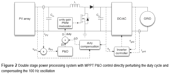
This paper is based on the work ''FPGA-based controller for mitigation of the 100 Hz oscillation in grid connected PV systems'', developed by the authors, which appeared in the 2010 IEEE International Conference on Industrial Technology (ICIT-2010, © 2010 IEEE), and it is focused on the FPGA-based implementation of an intuitive control strategy able to reduce the back- propagation of the low frequency (100/120 Hz) voltage oscillations from the dc-link capacitor to the source terminals. The technique is explained with reference to a PV system, but it can be applied to a fuel cell system in the same way. It operates by means of the predictive calculation of the duty-cycle correction required to keep the PV voltage at an almost constant value. The solution is based on the control scheme shown in Figure 2: the comparison with the scheme depicted in Figure 1 reveals that an additional block is used in order to compensate for the low frequency voltage oscillation.
FPGA devices are gaining a large application in the area of control of industrial systems and renewable energy systems [14, 15]. The main contribution of this paper is the efficient implementation of the predictive compensation technique in an FPGA device, in order to ensure the minimum use of hardware resources, reducing costs. So that, the largest number of the FPGA gates and multipliers are available for the implementation of the other control functions, e.g. the MPPT and the control loops of the dc/ ac stage. The proposed solution is described with reference to a boost converter used to step up the PV voltage to the level required by the inverter, and it was validated by means of experimental results obtained on a test bench based on a 200 W dc/dc boost converter and a photovoltaic array. Nonetheless, the approach can be applied to any dc/dc converter with the only difference that the design equations must be modified based on the conversion ratio of the adopted converter. Moreover, the conclusions drawn with reference to PV applications can be extended also to fuel cell systems. In the sequel, the European case characterized by the presence of a 100 Hz voltage oscillation is referred to, but similar results can be easily obtained in the US case characterized by a 120 Hz voltage disturbance.
Mitigation of the low frequency voltage oscillation at the PV array terminals
As anticipated above, the adopted technique is based on a suitable correction of the duty cycle value of the dc/dc converter, which is the first stage of the power processing system shown in Figure 2. The duty cycle D is calculated from the expression of the voltage conversion ratio of the boost converter as in (1), considering Continuous Conduction Mode (CCM) operation,
where VPV and Vo=Vb are the PV voltage, at the input of the boost converter, and the bulk voltage, at the output of the boost converter, respectively.
By neglecting the switching ripple and by operating in the low frequency range, the output voltage can be approximated as given in (2),
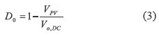
where Vo,DC and ΔVo are the DC component and the 100 Hz oscillation of the output voltage, respectively. By defining the steady-state duty cycle value D0 for the DC output voltage component Vo,DC as in (3),
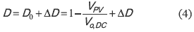
the mitigation of the voltage oscillation can be obtained by adding a duty cycle component ΔD calculated as given in (4).
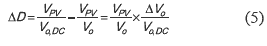
By combining equations (1) and (4), the correction that have to be imposed in order to compensate the oscillation ΔVo is given in (5), which ensures that the PV voltage remains almost fixed at a constant value.
A detailed analysis of such duty cycle compensator, demonstrating its stability, is given in [16].
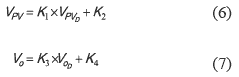
To provide an efficient implementation of the regulation strategy based on a FPGA device, the effect of the Analog-to-Digital Converters (ADC) used to acquire the PV and output voltages must be kept into account. The relations between the physical voltages and the digital data are given by the voltage sensors and ADC gains and offsets as in (6) and (7), where  and
and  are the digital representations of the PV and output voltages, respectively, and K1, K2, K3 and K4 are constants which are used to define the range of the measurements.
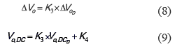
By using the superposition principle, the DC value and the low frequency oscillation component at 100 Hz of the output voltage can be determined using (9) and (8), respectively,
where  and
and  are the digital representations of the DC value and 100 Hz spectral component of Vo, respectively. Such relations allow to calculate the ΔD correction as given in (10), where the gain Kx is used to scale ΔD to the digital PWM (DPWM) word range [0, 2M-1], where M corresponds to the DPWM number of bits.
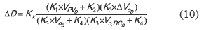
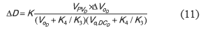
The adoption of a boost dc/dc converter, for which the operating constraint VPV < Vo holds, implies that the term K2, introduced to compensate the PV voltage sensor offset, is smaller than the offset term K4 and than the term  . Moreover, it is possible to adopt K2 = 0 by properly designing the associated signal conditioning circuitry. This approach is illustrated afterwards by means of the experimental results. Finally, by following the design criterion K2 = 0, ΔD is calculated as in (11), where K=Kx.K1/K3.
Efficient implementation of the compensation strategy on an FPGA device
The calculation of the ΔD value by means of (11) requires to define the desired value of the steady-state duty cycle D0; moreover, the 100 Hz frequency component must be obtained through a filtering procedure of the bulk voltage.
It is noted that the required 100 Hz filter can be implemented by means of IP cores from FPGA manufacturers, e.g. Xilinx LogiCORE IP FIR filter generator, or by means of VHDL code generated with Matlab or Labview software. However, such solutions use a large amount of gates and memory inside the FPGA due to its general-purpose design. In addition, the calculation of (11) and the 100 Hz filter require multiple multiplications and divisions, which are costly operations in terms of space realizations. Therefore, this paper proposes a custom realization for the 100 Hz filter, the ΔD calculation, and a divider, to provide an efficient FPGA implementation in terms of gates, memory, and multipliers. This condition permits to implement in a single and low cost FPGA device other functions required by a grid-connected photovoltaic system such as the MPPT algorithm and the control loops of the dc/ac stage.
Implementation of the 100 Hz digital filter
Instead of using an FIR filter realization as provided by multiple commercial design tools, this work adopts an IIR filter realization since it is computationally efficient in comparison with an FIR equivalent design and can be implemented in a single stage filter [17]. Therefore, IIR filters require less memory blocks and multiplicative operations in comparison to its FIR counterparts, which makes IIR realizations a suitable solution to reduce the amount of required FPGA resources.
The extraction of the 100 Hz component from the samples of the boost converter output voltage is performed through a second order IIR filter whose structure is given in (12) [18], where y[n] and x[n] represent the output and input samples, while ai and bi represent the filter coefficients.
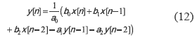
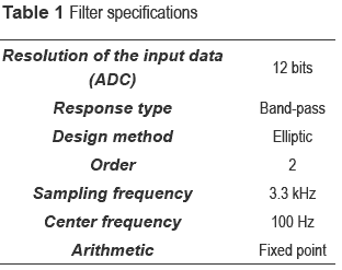
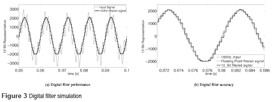
The analysis of the transfer function, the design and the calculation of its coefficients have been carried out by means of the Filter Design and Analysis Tool (FDATool) in Matlab. Any FPGA implementation requires to afford the problem of the fixed-point representation of the system parameters, namely the definition of the number of bits needed to represent the coefficients. On one side, the lower the number of bits the shorter the calculation time and the smaller the amount of hardware resources needed for the implementation. On the other hand, the larger the number of bits the greater the precision of the coefficients representation. The filter coefficients have been represented by using a resolution of 12 bits, which is equal to that one of the samples coming from the ADC used. Such a choice ensures a good trade off among complexity, amount of resources used for the implementation, accuracy in the representation of the filter coefficients, maximum achievable sampling rate and minimum transition bandwidth of the filter. Table 1 shows an overview of the specifications produced by means of the Matlab FDATool for the second order IIR band-pass filter with center frequency equal to 100 Hz, while in figure 3(a) the results of the Matlab simulations are reported considering the 12-bit fixed point coefficients and an input signal composed by 100 Hz and 500 Hz components, where a satisfactory filtering performance is observed. Figure 3(b) puts into evidence that the FDATool based procedure used for designing the parameters values listed in Table 1 has given a satisfactory fitting between the responses obtained by means of the floating point and 12-bit fixed point implementations of the filter coefficients.
The implementation of the IIR filter requires an increased complexity of the processing mechanisms in comparison to parallel and non-recursive FIR filters. In particular, the adopted strategy allows to use a single multiplier and a single adder to process all the filter operations, involving also a repeated and synchronized use of the same circuit block.
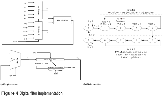
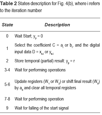
Figure 4(a) shows the logical scheme of the digital filter implementation employing a von Neumann structure [19]. In this implementation, the operands are obtained through a reference to two multiplexers. The first one provides to the multiplier the samples of the bulk voltage and of the PV voltage. The second multiplexer provides the values of the coefficients of the filter transfer function. The result of the product is stored and added (or subtracted, depending on the sign of the coefficients) to the next iteration product. Subsequently, the data at the input of the multiplexer are updated and the filtered data is available at the filter output. The flow control of the data in the digital filter is performed by the state machine described in Figure 4(b), were the processing of the k-th sample input at the k-th step begins with the rising of the start bit (S). Table 2 describes in detail each state of figure 4.
ΔD Generator module
The module for generating the correction ΔD is implemented by using the samples of the bulk and the PV voltages signals. Once again, in order to save hardware resources, the ΔD calculation has been divided into several sequential operations, at the cost of a negligible increase in the logic complexity. This goal is achieved by using two multiplexers handling the processing order of the operands involved in the different operations.
The logic scheme of the ΔD correction generator is depicted in figure 5(a). The samples of the output voltage are sent to a divider and to the digital filtering module, which extracts the 100 Hz component of the bulk voltage, at the same time. The constant K represents the sum of contributions related to the compensation of the value of the sampled data, in terms of offset and gain introduced by the ADC, and the compensation of the resolution in which the ΔD value must be represented (210 in this application). By addressing the first two operands, and constant K, they are available for processing and sent to the multiplier. The result of the multiplication is sent to the divisor module where a division by is performed. The output of the divider is sent back to the multiplexer input: it will be selected simultaneously with , which is the oscillation at 100 Hz calculated by the filter module, and those data are used for the second and final multiplication. The value of DC output voltage is described as a power of two to speed-up the calculation of the final expression of ΔD by performing the final division using a left shifting operation by a predetermined number of bits. The state machine that controls the ΔD correction generator is depicted in figure 5(b), and table 3 gives a description of each state.
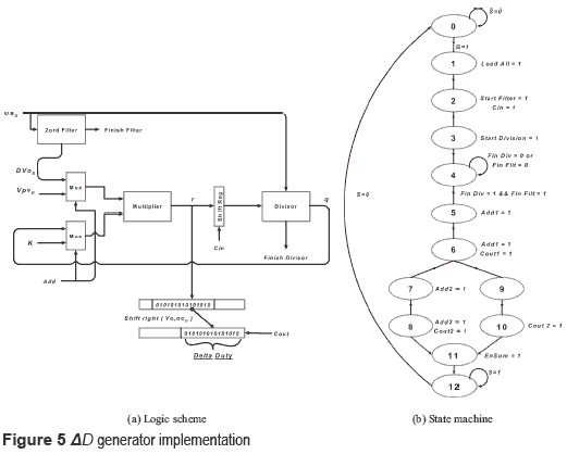
The sequence of sub-operations has been optimized to speed-up the process of development and taking advantage of the parallelization of part of the calculations required for ΔD with the ones required to perform the digital filtering.
Efficient-in-resources divider module
Traditional dividers have been avoided by DSP algorithm designers due to its complexity and cost of hardware implementation. Therefore, FPGA manufacturers have developed divider IP cores with high performance for integer division in terms of speed, e.g. Xilinx Divider Generator LogiCORE IP. However, such solutions use high level of parallelism to obtain fast processing, requiring a large amount of resources from the FPGA device. The need of a division between two positive numbers, as in (5), has required the development of an efficient in resources divider.
In the proposed implementation, three shift registers were used: the first one for the dividend, the second one for the divider, and the third one for the quotient. Even if the goal is to implement a circuit that allows the division between the 22-bit dividend and the divisor at 11-bits, in the solution presented in Figure 6(a) the registers are all at 22- bits in order to allow the overlapping bits of the divisor and the shifting to the right along all the bits of the dividend.
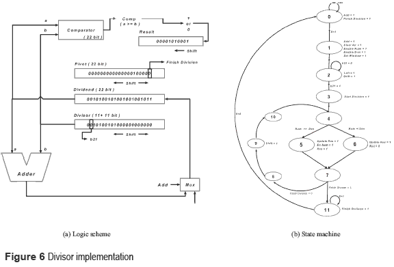
Once the values of the operands are loaded and the register containing the result is cleared, the bits of the divisor are shifted left, and correspondingly a zero is placed right in the register, so that the position of the most significant bit of the dividend overlaps with the most significant bit of the divisor exactly. The position ofthe least significant bit ofthe divisor is stored by using the 22-bit Pivot register, that is settled at the start to the hexadecimal value 2FFFFF (all bits settled to 1): any left shift of the divisor matches with one left shift and an insertion of a zero from the right of the pivot register, hence the position of the last ''1'' in the register corresponds to the position of the least significant bit of the divider. Each right shift is preceded by a comparison to determine if the dividend is greater than the divisor. If the dividend is greater than the divisor then the module performs the subtraction and the right shift of the bits of the divisor. The process ends when the least significant bit of Pivot reaches the zero position. In Figure 6(b) the state machine of the divisor module is presented; table 4 gives a description of each state function.
Experimental validation
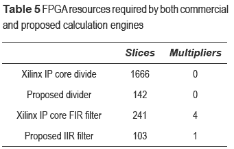
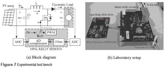
The proposed algorithm and calculation engines have been implemented by using the evaluation Board OPAL KELLY XEM3010 with an FPGA Spartan3 XC3S1500 [20], which has been also used to generate the PWM control signal for the dc/dc converter. To provide a measurement of the proposed implementation efficiency in terms of FPGA resources, table 5 presents the number of slices, which are elementary programmable blocks used to measure the resources allocated in Xilinx FPGAs including flip-flops and combinational gates [21], and multipliers required by both commercial (Xilinx IP cores) and proposed calculation engines. It is noted that the developed divider requires only the 8.52 % of the slices used by the Xilinx IP core divider, while the designed IIR filter structure requires only the 42.73 % of the slices and 25 % of the multipliers than its commercial counterpart. Hence, the complete ΔD calculation engine, including the filter and PWM generator, requires only 1066 slices and 2 multipliers, which are less slices than a single Xilinx IP core divider and less multipliers than a single Xilinx IP core FIR filter.
To experimentally validate the performance of the proposed solution in the reduction of the 100 Hz disturbances present in the bulk capacitor, a 200 W dc/dc boost converter has been designed and experimentally built up. The tests have been performed with two Kyocera KC120 PV modules connected at the converter's input and an electronic load connected at the converter's output. The electronic load was configured to simulate the dc/ac stage by imposing a dc voltage value Vo,DC equal to 200 V and a sinusoidal perturbation at 100 Hz with a peak-to-peak value ΔVo of 70 Vpk-pk, namely the 35 % of the dc value. In the experiments, a value Cb=22 μF and a PWM resolution Kx=210 were adopted. Moreover, the calculated 100 Hz filter coefficients were a0=160, a1=0, a2=-160, b0=1024, b1=-1696 and b2=703; and the adopted ADC coefficients were K1= 0.04, the desired condition K2=0 V, K3=0.23788 and K4=-189.53 V. Figure 7(a) shows the block diagram of the experimental test bench, and figure 7(b) shows the laboratory setup.
During the experimental test, the steady-state duty cycle value D0 has been chosen so that, at the current irradiation value, the input voltage has been settled at 40 V in the maximum power point. In other words, the MPPT algorithm has been disabled to evaluate the pure correction effect. During the test, the PV array current was higher enough to ensure that the boost converter was operating in CCM.
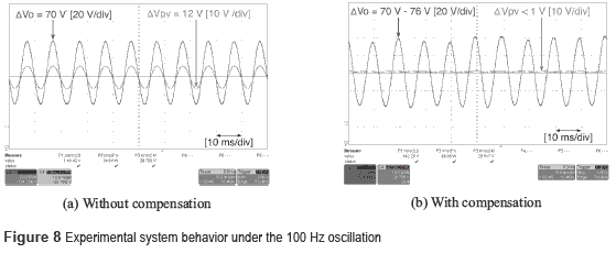
Figure 8 shows the bulk voltage and the PV voltage in presence of the 100 Hz oscillations at the converter's output. In particular, Figure 8(a) depicts the PV voltage without activating the 100 Hz compensation controller, with an oscillation amplitude of 10 Vpk-pk at least, which corresponds to 25 % of the desued MPP voltage. The effect of the proposed FPGA-based 100 Hz compensator can be appreciated in Figure 8(b), where the same bulk voltage oscillation imposed in the previous case, with additional DC-link oscillations at low frequency components generated by the electronic load operation, leads to a negligible PV voltage oscillation. This result demonstrates the satisfactory mitigation of the undesired bulk voltage oscillation by the proposed FPGA-based solution.
Conclusions
In this paper an FPGA-based solution to efficiently implement a control strategy aimed at reducing the source voltage oscillations at twice the grid frequency in single-phase inverters for renewable energy systems has been proposed. It consists in the analytical calculation of the duty-cycle compensation that can lead to a nearly constant source voltage. The FPGA implementation has been designed with the aim of minimizing the hardware resources employed for this function to allow its integration with additional MPPT or control algorithms in a single device. This characteristic permits to reduce costs by using a smaller and cheaper FPGA device to implement all the control algorithms of grid-connected systems in comparison to solutions based on commercial IP cores or analog 100 Hz compensators. Finally, the proposed approach has been validated by experimental results on a photovoltaic system, and its resources consumption has been contrasted with the ones required by commercial IP cores.
Acknowledgments
This work was supported by PRIN08 of University of Salerno, project VECTORIAL-MPPT of the Universidad Nacional de Colombia, and GAEI research group of Universitat Rovira i Virgili.
References
1. J. Lai. ''Power conditioning circuit topologies.'' IEEE ind. electron. Mag. Vol. 3. 2009. pp. 24-34. [ Links ]
2. S. Kjaer, J. Pedersen, F. Blaabjerg. ''A Review of Single-Phase Grid-Connected Inverters for Photovoltaic Modules.'' IEEE trans. on ind. appl. Vol. 41 .2005. pp. 1292-1306. [ Links ]
3. G. Petrone, G. Spagnuolo, R. Teodorescu, M. Veerachary, M. Vitelli. ''Reliability Issues in Photovoltaic Power Processing Systems.'' IEEE trans. on ind. electron. Vol. 55. 2008. pp. 2569-2580. [ Links ]
4. R. Gemmen. ''Analysis for the Effect of Inverter Ripple Current on Fuel Cell Operating Condition''. J. offluids eng. Vol. 125. 2003. pp. 576-585. [ Links ]
5. W. Choi, P. Enjeti, J. Howze, G. Young. ''An experimental evaluation of the effects of ripple current generated by the power conditioning stage on a proton exchange membrane fuel cell stack.'' J. of mater. eng. and perform. Vol. 13. 2004. pp. 257-264. [ Links ]
6. G. Spagnuolo, G. Petrone, S. Araujo, C. Cecati, E. Friis, E. Gubia, D. Hissel, M. Jasinski, W. Knapp, M. Liserre, P. Rodriguez, R. Teodorescu, P. Zacharias. ''Renewable Energy Operation and Conversion Schemes: A Summary of Discussions During the Seminar on Renewable Energy Systems.'' IEEE ind. electron. mag. Vol. 4. 2010. pp. 38-51. [ Links ]
7. R. Wai, C. Lin. ''Active Low-Frequency Ripple Control for Clean-Energy Power Conditioning Mechanism.'' IEEE trans. on ind. electron. Vol. 57. 2010. pp. 3780-3792. [ Links ]
8. M. Mohr, W. Franke, B. Wittig, F. Fuchs. ''Converter Systems for Fuel Cells in the Medium Power Range: a Comparative Study.'' IEEE trans. on ind. electron. Vol. 57. 2010. pp. 2024-2032. [ Links ]
9. N. Femia, G. Petrone, G. Spagnuolo, M. Vitelli. ''A Technique for Improving P&O MPPT performances of Double Stage Grid-Connected Photovoltaic Systems.'' IEEE trans. on ind. Electron. Vol. 56. 2009. pp. 4473-4482. [ Links ]
10. G. Tsengenes, G. Adamidis. ''Investigation of the behavior of a three phase grid-connected photovoltaic system to control active and reactive power.'' Electr. power syst. res. Vol. 81. 2011. pp. 177-184. [ Links ]
11. S. Buso, P. Mattavelli. Digital Control in Power Electronics. 1st ed. Ed. Morgan & Claypool. Sacramento, USA. 2006. pp. 109-144. [ Links ]
12. J. Kwon, B. Kwon, K. Nam. ''Grid-Connected Photovoltaic Multistring PCS With PV Current Variation Reduction Control.'' IEEE trans. on ind. electron. Vol. 56. 2009. pp. 4381-4388. [ Links ]
13. F. Ruz, A. Rey, J. Torrelo, A. Nieto, F. Canovas. ''Real time test benchmark design for photovoltaic grid- connected control systems.'' Electr. power syst. res. Vol. 81. 2011. pp. 907-914. [ Links ]
14 E. Monmasson, L. Idkhajine, M. Naouar. ''FPGA- based Controllers.'' IEEE Ind. Electron. Mag. Vol. 5. 2011. pp. 14-26. [ Links ]
15. J. Guerrero, F. Blaabjerg, T. Zhelev, K. Hemmes, E. Monmasson, S. Jemei, M. Comech, R. Granadino, J. Frau. ''Distributed Generation: Toward a New Energy Paradigm.'' IEEE ind. electron. mag. Vol. 4. 2010. pp. 52-64. [ Links ]
16. C. Ramos, G. Petrone, A. Saavedra. ''Compensation of DC-link voltage oscillations in grid connected PV systems.'' Rev. Fac. Ing. Univ. Antioquia. No. 63. 2012. pp. 82-92. [ Links ]
17. U. Farooq, H. Jamal, S. Khan. ''Transformation to implement computationally efficient IIR decimation filters.'' Digit. signal process. Vol. 19. 2009. pp. 33-44. [ Links ]
18. A. Oppenheim, R. Schafer, J. Buck. Discrete-Time Signal Processing. 2nd ed. Ed. Prentice Hall. New York. USA. 1998. pp. 465-478. [ Links ]
19. K. Rangarao, R. Mallik. Digital Signal Processing a Practitioner's Approach. 1st ed. Ed. John Wiley & Sons. New York, USA. 2005. pp. 101-119. [ Links ]
20. Opal kelly. XEM3010 User's Manual. Available on: http://assets00.opalkelly.com/library/XEM3010-UM.pdf. Accessed: December 2011. pp. 5-22. [ Links ]
21. Xilinx. Spartan-3 Generation FPGA User Guide - Extended Spartan-3A, Spartan-3E, and Spartan-3 FPGA Families. Aviable on: http://www.xilinx.com/support/documentation/user_guides/ug331.pdf. Accessed: December 2011. pp. 203-212. [ Links ]
