


Serviços Personalizados
Journal
Artigo
 Inglês (pdf)
 Artigo em XML
 Referências do artigo
 Enviar este artigo por email
Indicadores
-
 Citado por SciELO
 -
 Acessos
Links relacionados
-
 Citado por Google
 -
 Similares em
SciELO
Similares em
SciELO -
 Similares em Google
Compartilhar

 Permalink
Revista Facultad de Ingeniería Universidad de Antioquia
versão impressa ISSN 0120-6230
Rev.fac.ing.univ. Antioquia no.75 Medellín abr./jun. 2015
https://doi.org/10.17533/udea.redin.n75a11
ARTÍCULO ORIGINAL
DOI: 10.17533/udea.redin.n75a11
Graphene samples preparation and some possible uses in developing optical communication devices
Preparación de muestras de grafeno y algunos posibles usos en el desarrollo de dispositivos en comunicaciones ópticas
Juan Diego Zapata-Caro1,2*, Ana María Cárdenas-Soto1, Rodrigo Henao-Henao3, Eunezio Antonio Thoroh de Souza2
1 Grupo de investigación en Telecomunicaciones Aplicadas (GITA), Facultad de Ingeniería, Universidad de Antioquia. Calle 67 N.º 53-108. Medellín, Colombia.
2 Graphene and Nanomaterials Research Center (MackGraphe), Mackenzie Presbyterian University. Rua da Consolação, 900. São Paulo, Brazil.
3 Grupo de Investigación Óptica y Fotónica, Instituto de Física, Universidad de Antioquia. Calle 67 N.º 53-108. Medellín, Colombia.
* Corresponding author: Juan Diego Zapata Caro, e-mail: jdzapa@gmail.com
(Received October 2014; accepted April 06, 2015)
Abstract
Graphene is a two-dimensional material which has been attracting the attention of worldwide scientific community, motivated by their optical and electronic properties. There are different methods for obtaining graphene, however the micromechanical exfoliation process is the simplest and it allows samples with high quality to be obtained. In this paper, the preparation process of graphene flakes by exfoliation method and their characterization by Raman spectroscopy are shown. Moreover, some possible uses of graphene flakes applied to develop optical communication high speed devices are described.
Keywords: graphene, Raman spectroscopy, flakes and exfoliation method
Resumen
El grafeno es un material bidimensional que ha atraído la atención de toda la comunidad científica alrededor del mundo; este interés es motivado por sus propiedades ópticas y electrónicas. Existen diferentes métodos para obtener grafeno, sin embargo el proceso más simple para su obtención es exfoliación micro mecánica, este proceso permite muestras con alta calidad. En este artículo, se muestra el proceso de preparación de muestras de grafeno por exfoliación micro mecánica y se usa la espectroscopia Raman para su caracterización. También se describen algunos posibles usos del grafeno en el desarrollo de dispositivos de comunicaciones ópticas de alta velocidad.
Palabras claves: grafeno, espectroscopia Raman, exfoliación micromecánica
Introduction
With the isolation of graphene, a carbon allotrope which constitutes a completely two-dimensional one single atom-thick material, the research of new two-dimensional materials has attracted the attention of the worldwide scientific community.
This interest is motivated because of their electronics and optical properties of two-dimensional materials, which can be used for developing devices at nano-scale [1, 2]. The graphene has particularly two interesting properties: high electronic mobility with low temperature dependence and high optical transmittance. These properties make the graphene a very attractive material for the construction of high-speed optoelectronic devices [2, 3].
We mean by electronic mobility, the speed of the carriers in presence of an electrical field. This characteristic is significantly important for electronic devices; a high mobility means a faster switching in the transistor with the same applied voltage. For graphene, this mobility is greater than in silicon, opening the opportunity to build devices with higher switching speed, better electrical conductivity and lower heating [3].
Regarding near-infrared and visible transmittance, graphene has an absorption of 2.3% [1], which makes it ideal for the construction of optoelectronic devices, as it is practically transparent to these wavelengths. Besides, optical non-linear properties arise with the interaction between graphene and light [4]. This is very useful for designing different telecommunication devices such as: ultra-short pulse lasers, broadband modulators, antennas on the order of THz, and fiber-based optical devices. However, getting two-dimensional materials is a challenge itself.
There are different mechanisms for obtaining graphene, which vary from each other in quality, quantity, and purity of the collected samples. The process to obtain graphene from graphite is known as micromechanical exfoliation [3]. This technique consists in covering a graphite sample with Scotch tape and successively removing it. The effect on graphite is to break the Van der Waal ligations until obtaining only one monolayer material [2].
Once graphene flakes are obtained, it is necessary to identify them over the tape using an optical microscope; and to characterize them according to their electronic and optical properties a Raman spectrometer is used. For these processes, the graphene flakes on the tape are transferred over a SiO2/Si (Dioxide of silicon on silicon) substratum. The SiO2 thickness substrate is between 100 nm to 300 nm [5, 6]. The transference to this substrate allows a better optical contrast, in order to facilitate the graphene identification by optical microscopy using several filters. The contrast is originated by constructive interference, where the SiO2 acts as a filter, the Si acts as a mirror, and the graphene on the surface interacts with light, generating an optical contrast, thus allowing the graphene flake visualization.
In this paper, the preparation process of graphene flakes by exfoliation method is shown. The purpose is used this samples in the to develop of high speed telecommunication devices. In the first section, the exfoliation process is explained. This process was accomplished at the laboratories of Federal University of Minas Gerais in the Carbon Nanotubes Group. Subsequently, the characterization process using Raman spectroscopy is described and its application to three graphene samples is included. Finally, some applications in the optical communications field are presented.
Graphene flakes obtained through the micromechanical exfoliation technique
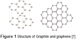
The micromechanical exfoliation process, also called Scotch Tape method [1, 7, 8], consists in breaking the Van der Waals ligations among graphite layers, as can be seen in Figure 1. Although it is a manual process, samples obtained with this technique have excellent characteristics. Nevertheless, it is very inefficient for large-scale production.
There are other ways previous for example: CVD (Chemical-Vapor-Deposition) [1], liquid phase exfoliation [1, 2], oxidation-reduction [1], carbon segregation and chemical synthesis [3], chemical exfoliation [1, 2], and graphene oxide [1]. Although these methods permit to obtain graphene to large scale, during the material growth phase, polycrystalline structures with several orientations could be presented, which could change significantly the electronic and optical properties. Giving that the micromechanical exfoliation allows getting better samples in terms of optical and electrical properties [2], this method is presented in detail as follows.
Steps to obtain graphene based on the micromechanical exfoliation process
The exfoliation process covers three phases: Preparation of the substrate where graphene will be deposited, micromechanical exfoliation to get graphene from graphite, and transference process of the graphene on tape to the prepared substrate.
Preparation of the substrate
The substratum commonly used for the exfoliation process is SiO2/Si (Dioxide of silicon on silicon), in this particular case, with a 300 nanometers thickness for SiO2. In order to obtain the maximum reliability, the substrate should be cleaned and dried. For this, the substrate was placed in a beaker with acetone and it was carried to an ultrasonicator for five minutes. For removing the acetone residue, the substrate was immersed in isopropyl alcohol, again it was placed in the ultrasonicator for five minutes, and then dried with nitrogen for 30 seconds. Finally, the sample was placed in a machine containing plasma gases such as oxygen and argon, for 10 minutes.
The O2 plasma was responsible for the cleaning and drying of the substrate. Silicon substrate with a polymer layer on top can also be used. The use of the polymer facilitates the transfer process of graphene to the substrate. In this particular case, the polymers used in the process are LOR and PMMA (polymethyl methacrylate). LOR is used because of its low viscosity for obtaining small films, with thicknesses of 100-1000 nm, depending on the rotation of the centrifugation equipment. Before applying the polymer, the substrate was cleaned and dried following the procedure detailed above. The substrate was placed in a centrifuge for applying two successive layers of polymer.
The following steps were utilized for each layer: 5 drops of polymer were put on the substrate; the sample was exposed to a rotation of 1000 rpm for 5 seconds to disperse the polymer on the substrate. Then the substrate was placed to a higher rotation of 3000 rpm for 40 seconds to control the thickness of the polymer film.
Micromechanical exfoliation process
For the exfoliation process, an adhesive tape of Semiconductor Equipment Corp. –Blue Medium Tack was used, because it leaves less residues in the sample. The graphite used was from the Nacional de Grafite Company, located in Minas Gerais, Brazil. The quality of the graphite is essential for larger exfoliated graphene flakes and to improve the contrast. The process was relatively simple: the tape was put on the graphite sample and the, pulled and place on the graphite sample in a repetitive way. The graphite layers were untied until the sample turned less dark.
Transferring the graphene to the substrate
The transfer consists in depositing the graphene exfoliated on the substrate SiO2/Si. This process is different if silicon with a layer of dioxide of silicon is used, or if a polymer film is added. For the first case, the tape set with graphene and substrate was exposed to a weight of 5kg for 10 minutes, in order to achieve better adhesion between the surfaces of the tape with exfoliated graphene and the substrate. For the second case, the substrate with polymer was placed on a stove at 2000C for 5 minutes, in order to harden the polymer with the added graphene.
After the flakes were transferred, the following step consists in their identification and characterization. These processes are very important to determine if a flake is constituted by either monolayer or multi-layer graphene. The opto-electronic properties of graphene, such as high electronic mobility, are determined by the number of layers and the quality of graphene.
Identification and analisys of graphene flakes
The samples obtained were identified and characterized by an optical microscope and Raman spectroscopy. The details of these two processes are as follows.
Identification of samples using optical microscope and filters
The identification of the different substrates was performed by means of an optical microscope OLYPUMS BX 51M, using an orange filter and a lens of magnification 50X. With this method, some samples of graphene deposited on Si/SiO2 were identified.
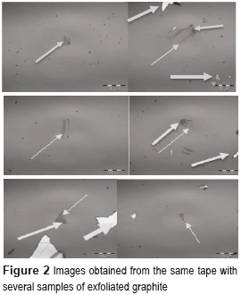
To locate the graphene sample, the substrate was observed with a gradual approach to locate the area where the graphene was. Once the position of graphene sample was established, your coordinates X and Y were registered. As a reference for the coordinates, images of the edge of the substrate were taken. All images shown in Figure 2, belong to the same sample, which exhibits monolayer, bilayer and multilayer. The monolayer graphene is the clearest (thin arrow), followed in intensity by bilayer graphene (medium thick arrow), and the (thicker arrow) corresponds to a multilayer graphene.
Samples analysis using Raman spectroscopy
Raman spectroscopy is a powerful tool for the characterization of physical and chemical properties of many materials. Raman spectroscopy is based on the analysis of the light scattered by a material when a beam of a monochromatic light impinges on it [7, 8].
The Raman spectrometer used in the analysis of samples is an Alpha 300 R Confocal Raman Microscopy System. For the analysis, the equipment has three continuous wave (CW) lasers in: 488 nm, 532 nm and 633 nm. The lasers have a maximum power of 30 mW, 41mW and 25 mW, respectively. In our case, the analysis was carried with the laser emitting in 488nm, and the power used was of 5mW. For focusing the sample, the Raman microscope, which is confocal and has three lenses 10X, 50X and 100 X, was used. The light collected in the reflection was guided by a multimode-mode fiber and detected by a CCD camera for photon counting. Only one of 106 photons scattered experienced inelastic scattering, generating the Raman effect, which was observed in the spectrum. From the Raman spectrum, it is possible to differentiate among graphite, monolayer graphene, bilayer graphene, and amorphous graphene; depending on the number of layers of the samples [7], they exhibit changes in relative intensity, in form and in line width.
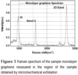
In Figure 3, a Raman spectrum of the graphene, which was obtained by the exfoliation process, is shown. The bands G and 2D are characteristics for graphene.
The relation between intensities of these bands I(2D)/I(G) provides information about the number of layers [7]. If I(2D)>I(G), the sample corresponds to a monolayer graphene; if I(2D)≤I(G), then the sample analyzed is bilayer or multilayer graphene. The full-width at half-maximum (FWHM) of the band 2D can also give information about of graphene monolayer. If the width is about 30 cm-1, then the sample is monolayer graphene; if the width is of 35 cm-1, then it is bilayer or multilayer [7].The characterization of three samples obtained at the Federal University of Minas Gerais labs are presented and based on information by the Raman spectrometer, considering the relation of intensities and the 2D bandwidth.
Sample number 1
Figure 4a, presents a contrast intensity map for a sample with different exfoliated graphene flakes. It is possible to see differences in the brightness intensities of flakes: the brightest zones correspond to a monolayer graphene and the darkest areas to a bilayer or multilayer graphene. The Raman spectrum in a point of the brightest zone is visualized in Figure 4b, where it is possible to observe that I(2D)>I(G), confirming the presence of monolayer graphene in this area. Figure 4c shows a profile of the relation between the intensities I(2D)/I(G) across the area comprised by the sample under analysis. The profile allows locating the zones where monolayer graphene is. When the relation between I(2D)/I(G) is greater than one, this indicates that monolayer graphene is present, otherwise the graphene is multilayer.
Samples number 2 and 3
In Figures 4d and 4g, the map of contrast intensities shows the zones with monolayer graphene and multilayer graphene. As mentioned above, the brightest areas correspond to monolayer graphene and darkest areas to bilayer or multilayer graphene. Figures 4e and 4h, show the Raman spectrum for the brightest area indicated by arrow 1. The corresponding spectrum, indicates the relation between the intensity of the bands, being I(2D)>I(G) as corresponds to monolayer graphene. On the other hand, in Figures 4f and 4i, the spectrum is shown for opaque zones marked with arrow 2, corresponding to a multilayer graphene.
In this case, the relation between the intensities is I(G)> I(2D). Finally, the 2D bandwidth is very important for completing the samples characterization.
Also, the 2D bandwidth allows identifying the number of layers. If the 2D bandwidth is in the order of 30 cm-1, then it is monolayer graphene; if 2D bandwidth is in the order of 40 cm-1, then it is multilayer graphene. In Figure 5, it is possible to see the 2D bandwidth map of sample 1. The black shades represent 2D bandwidth between 30 cm-1 and 35 cm-1 corresponding to a monolayer graphene. Meanwhile, dark gray shades indicate 2D bandwidth around of 40 cm-1 and 50 cm-1 indicating that in these zones, multilayer graphene is present [7]. The 2D bandwidth maps of the samples 2 and 3 can be observed in Figure 5. Once the monolayer graphene was identified and located, its transfer should be made to elements commonly used in optical communication systems, such as connectors and fiber segments.


Transfer of graphene to optical communication system elements
To take advantage of the optical properties of graphene for optical communication systems, it is essential to have a good transference method of graphene flakes to devices easily integrated to these systems [1, 9]. In order to improve the interaction between graphene and the optical signal, the size of the flake is very important, because it is desirable to cover completely the receptor surface with the graphene to be transferred. So, exfoliated samples of the order the 40 μm2, can be transferred to an optical connector, which core diameter is around 10 μm. However, there are configurations where graphene has a better interaction with the optical signal, for example the D optical fiber [10, 11]. The D optical fiber is an optical fiber that has been modified by removing a portion of the cladding as shown in Figure 6. For this configuration, graphene flakes of the order of 120 μm long are needed. These fibers improve the interaction of graphene with light, through of evanescent waves. The difficulty lies in getting larger flakes by micromechanical exfoliation, so the employed graphene is obtained by using the CVD technique.

Examples of graphene applied in optical communications systems
Once graphene flake is transferred on a device such as a connector or a fiber in D configuration, it is possible to use it in different optical communication applications.
Short pulse generation
One of the most remarkable applications of graphene is as saturable absorber (SA) in the generation of ultrafast femtosecond pulses. The generation of ultrafast femtosecond pulses has a great interest in the area of optical communications, since its broad spectrum can be used as an Optical Frequency Comb Generator, and in a single frequency, a high speed OTDM. A low cost mechanism for the generation of ultrafast femtoseconds pulses is the EDFL (Erbium-Doped-fiber Laser),this kind of device uses the Erbium as gain medium and the graphene as passive saturable absorber. In this device, the graphene filters low intensities and allowed passing the higher intensities, generating ultrashort pulses through a feedback in the closed cavity [12]. In Figure 7, a configuration (EDFL) using graphene is shown.

Broadband polarizer based on graphene
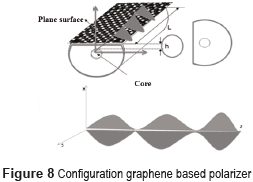
Fiber-based polarizers have shown their effectiveness in optical communications systems [10]. This type of polarizer works by selective coupling of the polarization between the evanescent field and a metal or a birefringent crystal. When the graphene is used, its electromagnetic response is very different to other metals, due to its optical conductivity. In fact, the conductivity in the metals is described by σ(ω,T) = σ' + jσ'', where the imaginary part of the conductivity σ'' ,can be positive or negative, depending on the frequency and the chemical potential, μ, which determines the kind of propagation mode in the surface. For example, in metals, the propagation mode is always TM. In the case of graphene, the conductivity can be determined by the interband and the intraband transitions σ(ω,T) = σintra(ω,T) + σinter(ω,T). The imaginary part of the intraband conductivity is always positive, allowing the TM mode propagation in the graphene film. The imaginary part of interband conductivity can result in negative values, providing the conditions for TE propagation mode. Consequently, unlike metals, graphene can support transverse electrical surface waves TE or transverse magnetic TM, depending on whether σ'' is positive or negative [10].
In Figure 8, a polarizer with graphene which uses D optical fiber is shown. The graphene allows the mode TE propagation, acting as filter for TM mode [10].
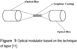
Optical modulator
Another important application of graphene is as an optical modulator. The graphene property used in this case is the optical absorption. Absorption can be controlled by a potential difference, which changes the Fermi level in the structure of graphene, modifying its optical transitions. This property allows using the graphene as an active medium for optical modulators based on optical electro absorption [13].
Another modulation mechanism is shown in Figure 9, in which a taper can be seen. The taper is a segment of fiber over which graphene is placed. The taper is obtained when the diameter of the optical fiber is diminished, in order to get more interaction between light and graphene deposited on the taper. When the wave passes through the adhered graphene, it undergoes a significant attenuation due to the graphene absorption. When a switching light is introduced inside the taper, the graphene carriers are excited and the graphene absorption threshold shifts to higher frequency levels, causing that the signal attenuation diminishes significantly. Thus, the switching light controls the modulation. This configuration allows easy integration to the optical network [11].
Conclusions
The graphene is a two-dimensional material with optoelectronic properties of great importance for application in the optical communication field. Due to its size, we need special instruments with high resolution for its identification, location, and characterization. We presented the processes of obtaining, identifying and characterizing micromechanically exfoliated graphene flakes. By Raman spectroscopy, two elements were used for the characterization: The relation between the intensities of the bands I(2D) and I(G), and also the band full-width at half-maximum (FWHM) of the band 2D. With Raman spectroscopy, it is possible to have a criterion for systematic evaluation in identifying graphene monolayer and multiple layers.
Monolayer graphene has important opto-electronic characteristics that are useful in optical communication applications, among them the generation of ultrashort pulses, broadband polarizers and optical modulators.
Acknowledgment
This Research was funded by the Universidad de Antioquia through of the CODI project MDC 11-1-06 and Sostenibilidad 2014 project. Ana Maria thank to the project COL 10-2-05. We thank the program Enlaza Mundos Medellín-Colombia, Mackenzie Presbyterian University and Federal University of Minas Gerais.
References
1. F. Bonaccorso, Z. Sun, T. Hasan, A. Ferrari. ''Graphene photonics and optoelectronics''. Nature photonics. Vol. 4. 2010. pp. 611-622. [ Links ]
2. H. Raza. Graphene Nanoelectronics: Metrology, Synthesis, Properties and Applications. 1st ed. Ed. Springer. Berlin, Germany. 2012. pp. 598-599. [ Links ]
3. A. Geim, K. Novoselov. ''The rise of graphene''. Nature Mater. Vol. 6. 2007. pp. 183-191. [ Links ]
4. M. Glazov, S. Ganichev. ''High frequency electric field induced nonlinear effects in graphene''. Physics Reports. Vol. 535. 2014. pp. 101-138. [ Links ]
5. P. Blake, E. Hill, A. Castro, K. Novoselov, D. Jiang, R. Yang, T. Booth, A. Geim. ''Making graphene visible''. Applied Physics Letters. Vol. 91. 2007. pp. 1-3. [ Links ]
6. A. Castro, F. Guinea, N. Peres, K. Novoselov, A. Geim. ''The electronic properties of graphene''. Reviews of Moderns. Vol. 81. 2009. pp. 109-160. [ Links ]
7. L. Malard, M. Pimenta, G. Dresselhaus, M. Dresselhaus. ''Raman spectroscopy in graphene''. Physics Reports. Vol. 473. 2009. pp. 51-87. [ Links ]
8. K. Novoselov, A. Geim, S. Morozov, D. Jiang, M. Katsnelson, I. Grigorieva, et al. ''Two-dimensional gas of Massless Dirac Fermions in Graphene''. Nature. Vol. 438. 2005. pp. 197-200. [ Links ]
9. H. Rosa, E. Souza. ''Bandwidth optimization of a Carbon Nanotubes mode-locked Erbium-doped fiber laser''. Opt. Fiber Technol. Vol. 18. 2012. pp. 59-62. [ Links ]
10. Q. Bao, H. Zhang, B. Wang, Z. Ni, C. Lim, Y. Wang, et al. ''Broadband graphene polarizer''. Nature Photonics. Vol. 5. 2011. pp. 411-414. [ Links ]
11. W. Li, B. Chen, C. Meng, W. Fang, Y. Xiao, X. Li, et al. ''Ultrafast–all optical graphene Modulator''. Nano Lett. Vol. 14. 2014. pp. 955-959. [ Links ]
12. W. Cho, J. Kim, H. Lee, S. Bae, B. Hong, S. Choi, et al. ''High-quality, large-area monolayer graphene for efficient bulk laser mode-locking near 1.25 μm''. Optics Letters. Vol. 36. 2011. pp. 4089-4091. [ Links ]
13. M. Liu, X. Yin, E. Ulin, B. Geng, T. Zentgraf, L. Ju, et al. ''A graphene-based broadband optical modulator''. Nature. Vol. 474. 2011. pp. 64-67. [ Links ]
