


 Inglês (pdf)
 Artigo em XML
 Referências do artigo
 Enviar este artigo por email
 Citado por SciELO
  Citado por Google
  Similares em
SciELO
Similares em
SciELO  Similares em Google
 Permalink
1. Introduction
The simultaneity of two physical properties such as electrical conduction and optical transparency occurs only in few systems such as SnO2 and InO3, which are characterized by having a 4d configuration 1)(2. Transparent conductive oxides (TCOs) have a lot of applications in optoelectronic devices such as (LEDs), transparent electrodes and buffer layers in solar cells, touch screens, buffer and as raw materials for varistors 3)(4)(5)(6)(7)(8)(9.
The high conductivity of several transparent oxides, has been explained as the result of point defects in the crystal lattice. Some authors argue that the reason for coexistence of the conductivity and transparency is related to the presence of shallow donor levels near the conduction band, formed by a large concentration of oxygen vacancies Vo 2. However, other theoretical results predict that interstitial tin plays a more prominent role than Vo; the oxygen vacancies produce deep levels in the energy gap, but the outermost electrons of interstitial tin produce surface levels within the conduction band, generating a higher amount of charge carriers 1.
The most reported TCO in literature is the Indium tin oxide ITO, but due to the high cost of Indium and the fact that it is ranked as 7.6 (being 9.5 the maximum) in the British Geological Survey risk list 2012 10, in recent years research in alternative TCOs has been intensified 11. SnO2 is a good prototype for TCO, since it has a larger energy gap of 3.6 eV and is a material with a transparency above 80% in the visible range 1. Thin oxide SnO2 occurs in nature as the mineral cassiterite, which is normally associated with pegmatitic rocks 12. The most stable phase of SnO2 has a tetragonal crystal structure that belongs to the group of rutile, which does not have close packing. Each tin atom is bound to 6 oxygen atoms at the vertices of an octahedron, and each oxygen atom is accompanied with 3 tins coplanar, forming approximately an equilateral triangle 13.
At room temperature it has a formation energy of 1.9* 103 J mol-1 and a heat capacity Cp = 52.59 J mol-1K-1. The density of tin oxide has an approximate value of 6.95 g cm-3, with a melting point of 1630° C and a hardness of 6-7 on the Mohs scale 13)(14.
The electrical conductivity of SnO2 and other physical properties can be improved and affected by the presence of doping elements such as F, Sb, V, Ta, Nb [15-18]. Especially the charrier density can be increased when the tin oxide is doped with niobium, because it has oxidation states of +3, and +5, and the tin oxidation states are +2, +4, making an additional charge carrier on conduction band 19.
There are many experimental techniques available to prepare undoped and doped SnO2, such as pulser laser deposition, spray pyrolysis, reactive evaporation, and sputtering 20)(21)(22. The sputtering technique is very controllable, reproductible and has high growth rates.
Many papers have described the effect of Nb doping on the physical properties of SnO221)(22)(23. However, in this paper a systematic analysis is presented of the variation of the structural, optical and electrical properties of Sn1-xO2Nbx thin films deposited by magnetron-sputtering technique, by changing the deposition power.
2. Experiment
To make the target, the synthesis of bulk material was performed by Pechini method according to literature 24. Doping was carried out in the solubility limit of 10% w/w. SnCl2 and NbCl5 were used as the source of Sn and Nb, respectively. Ammonia was used in the process to control the pH. Drying was done at 400oC and the calcination of the resulting powders was carried out at 600oC.
The obtained material was pressed into a disk of diameter d =2.54 cm and a thickness t = 0.3 cm, applying a pressure of 51714 Torr on 8g of Sn0.9O2Nb0.1 over 10 minutes, this disk was sintered at 800o C for 24 hours to obtain a pellet.
Sn1-xO2Nbx films were grown by RF-sputtering. The substrate used was alkali-silicon oxide (glass) which was previously sonicated in acetone.
To identify the influence of power deposition in the electro-optical properties, the films were grown at 35, 45, 50 and 55 Watts, keeping the pressure fixed 6.3*10-2 Torr with pure Ar, and deposition time of 2 hours. All the samples were grown at 350 oC, and the distance target-substrate was kept constant at 7.5 cm.
Structural characterization was performed using X-ray diffraction (XRD). The diffraction patterns were measured on a PANALYTICAL EMPYREAN with Cu(Kα), the wavelength of the radiation was λ=1.5418 Å, a pitch of 0.03o and a range of 10 to 80 in 2θ. Scanning Electronic Microscopy (SEM) JEOL JSM-6490LVwith (EDX) was used to check the presence of tin and niobium in the samples, Atomic Force Microscopy NANOSURF SCAN, was used to investigate the surface morphology.
Electrical resistivity measurements were made by the traditional method of Van-der-Paw, using a current source 236 KEITHLEY, and nanovoltimeter KEITHLEY 181. For electrical contacts silver paint was used.
The optical characterization was performed by using a Cary 100 VARIAN spectrophotometer, in a range of 300 to 800 nm.
3. Results and discussion
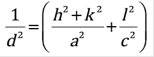
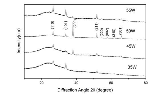
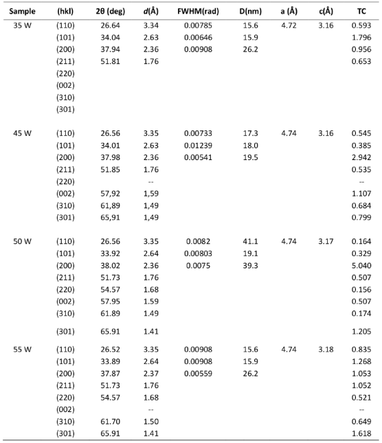
Figure 1 shows the diffractogram for the films deposited at different powers. The most significant peaks with the corresponding crystalline planes are also shown. The background of the diffractograms from 10o to 30o is typical of amorphous glass. The peaks for all films correspond to the characteristic peaks of tetragonal rutile SnO2 (standard ones from JCPDS card no. 41-1445). Non-secondary phases corresponding to niobium oxide 25, or SnO were found in the diffractograms. The lattice constants a and c of the tetragonal structure were determined by the following relation (1) 22:
 (1)
(1)
Where d is the interplanar distance and h, k and l are the Miller indices. The calculated lattice constants are given in Table 1. The calculated a and c values are slightly different than JCPDS card no. 41-1445 (a= 4.7382 Å, c = 3.1871 Å). The observed d values are presented in Table 1 and these values are compared to the standard. From Table 1, it can be observed that the lattice parameters are not very affected by the change in the power deposition.
The crystallite size D of the films from the XRD data was calculated using the Debye-Scherrers formula (2) 26
 (2)
(2)
Where β is the full-width at half of the peak maximum (FWHM) in radians and θ it is Bragg’s angle. Table 1 shows the values, and Figure 2(a) shows how the sample deposited at 50 Watts presented much higher crystallite size values in all the main planes (110), (101) and (200) compared to the samples deposited at other powers as is shown in the Figure 2(a). The average crystallite was 19.2 nm, 18.1nm, 33.16 nm, 19.2 nm, to the films deposited at 35, 45, 50, 55 Watts respectively.
The reflection intensities from each peak contain information related to the preferential or random growth of polycrystalline thin films, which is studied by calculating the texture coefficient TC(hkl) for the planes using the Eq. (3) 21.
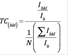 (3)
(3)
Where I(hkl) is the measured intensity of x-ray reflection, I 0(hkl) is the corresponding standard intensity from JCPDS data card no. 41-1445 and N is the number of reflections observed in the XRD pattern. The calculated TC values are presented in Table 1. A sample which has randomly oriented crystallites presents TC(hkl) = 1, but for larger values, the larger the abundance of crystallites oriented at the (hkl) direction. It is worthy to notice that the sample deposited at 50 Watts presented the largest texture coefficient TC for the plane (200) referred to all the other planes for the other samples. On the other hand, in the Figure 2(b) can be seen how the growth of the films in the direction (200) increases with increasing deposition power up to 50 Watts, then when increasing the power up to 55 Watts the orientation in that plane is significantly lower. The growth in the plane (101) decreases at 50 Watts and then it increases again at 55 Watts. The plane (110) did not present significant changes.
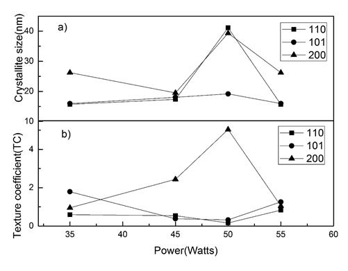
Figure 2 a) Variation of the crystallite size and b) Variation of the TC values of Sn1-xO2Nbx films with power deposition
The films grown at a) 35 Watts, b) 50 Watts c) 55 Watts exhibited granulate and homogeneous surface, see Figure 3. By using the software WsXM [27] and taking profiles of various grains in each sample, a grain size of 200 nm average was obtained. These values are higher than values of the crystallite size obtained by XRD, which suggests that each grain may contain several crystallites. The roughness average of the thin films was 4.8 nm, 4.3 nm and 4.5 nm respectively, with an insignificant difference in the roughness of the films. Those values represent smooth films as expected by sputtering.
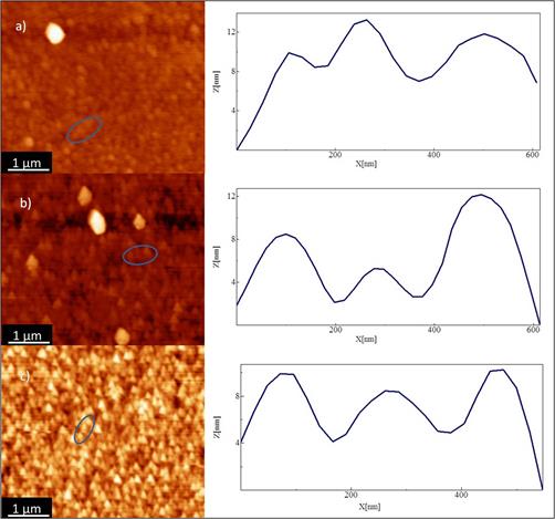
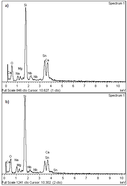
Figure 4 shows the EDS peaks for the oxygen, tin, and niobium content. Silicon, calcium and magnesium, belong to the glass substrate. The presence of Nb together with the X-ray diffraction patterns, in which no clear evidence of secondary phases and the change in the values of the lattice parameters respect the standard values, suggests that there was incorporation of niobium in the crystalline structure of the films. The analysis for the atomic percentage of each element presented in the sample can only be performed in a qualitative manner, since oxygen is present on the surface of the film, in the film, and in the substrate, which makes it impossible with EDS determine the final stoichiometry in the samples. The EDS for the other films do not show additional information and therefore are not presented here.
The resistivity of the material decreased when the deposition power increases to a power limit of 50 Watts, see Figure 5. At this point, resistivity starts slightly to increase, this agrees with the trend of samples to grow preferentially in the direction (200) when the deposition power is increased, and with the fact that the films have a larger crystallite size in this plane, as seen in Figures 2(a) and 2(b). This preferential growth in a particular direction allows a decreasing in the crystallite boundaries which leads to decrease the potential barriers presented by changing the crystallographic orientation. In the crystal boundary, defects find favorable habitat due to dislocations caused by the crystallographic mismatch, allowing different ions with different charge states 28)(29, these ions can belong to the host material (Sn, O), or dopant material (Nb). When there are chemical species in the grains boundaries, there are not changes in the crystallographic phase of the material (therefore no other phases are observed in the XRD patterns), but these species generate potential barrier (resistance) in intergrain interfaces, which limits carriers transport; therefore, while smaller grains or crystals are held, the electron mobility decreases and hence its conductivity, although the number of charge carriers is not affected. The explanation of change in crystallite size by varying the power deposition is that power deposition modifies the arrival energy of atoms and ions to the substrate, changing the energy of diffusion of atoms 30, which leads to different formation of crystals and defects grains. Therefore, there is an optimum power deposition which maximizes crystallite size.
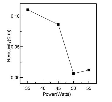
Figure 6 shows the transmittance for the films. The sample grown at 35 Watts presented a transmittance greater than 98 % in the region between 450 nm and 800 nm. This result coincides with the low crystallinity and low conductivity of the sample. The transmittance decreases for wavelengths less than 450 nm for the violet and ultraviolet regions. The sample grown at 45 Watts showed a transmittance up to 90 % in the region of 550 nm (green), the maximum transmittance greater than 98 % occurred in the region above 700 nm corresponding to red region. Similar features were found for the samples grown at 50 and 55 Watts.
The samples showed a transmittance above 85 % in the visible region, except for the violet. These optical properties make it very attractive for optoelectronic devices, especially those that require sunlight, since the greatest emission belongs to the region between 550 and 650 nm. The films deposited at 45, 50 and 55 Watts have interference fringes due to the light passes from the film to the glass substrate.
The occurrence of these interference fringes is also a test of the smoothness and homogeneity of the surface, as when the sample is very rugged, the interference phenomenon does not occur due to the scattering 31.
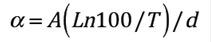
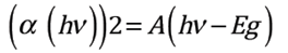
According to 32, the absorption coefficient can be defined as shown in Eq. (4) where T is transmittance and d is the film thickness. The coefficient is related to energy according to Eq. (5). The interpolation of the linear region of the graph of the absorption coefficient vs energy gives the energy gap (Eg) of Sn1-x O2Nbx films as shown in the inset of Figure 6.
 (4)
(4)
 (5)
(5)
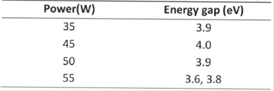
Table 2 shows the energy gap for films grown at different powers. The thickness of the films measured by AFM were from 150 nm to 200 nm. It is observed that the energy gap for the samples deposited at (35, 45 and 50) Watts, are in the ultraviolet region between 3.9 eV and 4.0 eV, but the sample grown at 55 Watts shows two lineal regions, in one of then the gap is 3.6 eV in the other the gap is 3.8 eV, it could be for the presence of different charge states of Sn. The energy gap of the SnO2 has some different values as reported in the literature 33. This difference can be explained by the multi-valence of tin. So the films can contain SnO2 and SnO 33, but in this case, as observed from the XRD analysis, the SnO phase was not found.
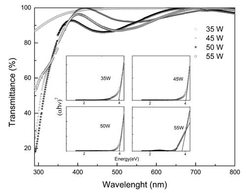
Figure 6 Optical transmittance spectra of Sn1-xO2Nbx thin films, the inset shows the energy gap for the films
4. Conclusions
Polycrystalline Sn1-xO2Nbx thin films were grown on glass substrates by varying the power deposition. The results showed that the Sn1-xO2Nbx films increased their electrical conductivity when the deposition power is increased. A strong dependence on the crystallite size and crystallographic planes orientation was obtained upon variation of power deposition. Conductivity of the films increases as the films grow preferentially in orientation (200). The energy gap reached a minimum value of 3.6 eV. All films were transparent in the visible range, with a transmittance greater than 80%. The results confirm the importance of power deposition to obtain controlled and smooth thin films of Sn1-xO2Nbx and their potential for being used as buffer layers or transparent conductors for opto-electronic devices applications.

