


 English (pdf)
 Article in xml format
 Article references
 Send this article by e-mail
 Cited by SciELO
  Cited by Google
  Similars in
SciELO
Similars in
SciELO  Similars in Google
 Permalink
1. Introducción
The recent emergence of hybrid perovskite materials with the general formula AMX3 (A=Cs+, CH3NH3 +, or HC(NH2)2 +; M=Pb2+; and X=Cl-, Br-, and I-) has attracted the attention of numerous academics within the photovoltaic field in recent years, since the first report of Kojima et al.[1] in 2009. The three-dimensional (3D) methylammonium (MA) lead iodide (MAPbI3) is the most promising material to achieve solar cell devices with high performance[2] [3] [4] [5]. The main advantages of this material are related to its exceptional properties as an adequate solar cell absorber, including small exciton binding energy[6], high extinction coefficient[7], adequate band gap[8], and long exciton and charge diffusion lengths[9].
Nevertheless, there are two main drawbacks in the future development of lead-based perovskite devices: the degradation of the material by atmospheric moisture[10] and the toxicity of the resulting lead[11]. Improving the moisture stability of the material can also help to reduce the impact of lead toxicity because it could prevent the water-soluble perovskite from easily dissolve. Replacing MA with formamidium (FA) has resulted in better thermal stability, but not in better moisture stability[12] [13]. Nevertheless, there is a broad range of less water-soluble organic cations that can be used to replace MA. But, these larger cations exceed Goldschmit’s tolerance factor that determines the formation of 3D perovskite[14] [15]. However, two-dimensional (2D) stable perovskite structures are also easy to obtain. Among these 2D stable perovskites are the Ruddlesden-Popper layered perovskites with the general formula A2Bn-1PbnI3n+1, which can go from simple 2D (n=0) to 3D (n=∞).
Cao et al.[16] investigated the 2D Ruddlesden-Popper (BA)2(MA)n−1PbnI3n+1 layered perovskite where BA corresponded to the n-butylammonium cation CH3(CH2)3NH3 +. They found improved moisture stability for the best photovoltaic device with an efficiency of 4.02% when n=3. Later, in the same system, Tsai et al.[17] Carried out a hot casting method to achieve a better orientation of the films, which allowed them to increase from 4.44% to 11.44%. Similar 2D Ruddlesden-Popper systems were also investigated using phenylethylammonium cation, PhC2H5NH3 + (PEA) in the (PEA)2(MA)2Pb3I10 system; the resulting devices showed improved moisture stability and efficiencies ranging from 4.73% to 7.02% that highly depended on the scan rate (indicating hysteresis)[18].
It is important to notice that there is still a lot of work to develop regarding the layered perovskite structure considering the options in terms of the value of n and the multiple organic cations combination[19]. The previous works concluded that the most promising system for 2D Ruddlesden-Popper layered perovskite is obtained when n=3[20]. These results should be taken as an initial point to keep improving the stability and performance of these new layered systems in order to contribute to the faster development of lead hybrid perovskite solar cells. The right choice of the organic cation in these systems determines the final properties of the active layer since large cations with lower polarity can improve the moisture stability but can also affect the transport properties across the organic chains. Therefore, in this work, we investigate and report the fabrication and properties of 3D MAPbI3 and 2D Ruddlesden-Popper layered perovskites with n=3. Three organic cations of different nature, such as n-propylammonium (PA), t-butylammonium (BUA) and benzylammonium (BEA) were selected to obtain the three-layered perovskites (PA)2(MA)2Pb3I10, (BUA)2(MA)2Pb3I10 and (BEA)2(MA)2Pb3I10. Due to differences in hydrophobicity, size and structure, all materials showed very dissimilar photovoltaic properties, but in all cases improved moisture stability compared to the 3D MAPbI3 perovskite. Different from PA and BEA, the shorter branched BUA cation allowed adequate moisture tolerance and better transport properties for the (BUA)2(MA)2Pb3I10 system.
2. Experimental methods
2.1 Perovskite synthesis
Methylammonium iodide (MA), Propylammonium iodide (PA), t-Butylammonium iodide (BUA), and Benzylammonium iodide (BEA) from Dyesol were used as organic cations. Dimethyl sulfoxide (DMSO, Sigma Aldrich) and dimethylformamide (DMF, Alfa Aesar) were used as solvents, and lead iodide (Alfa Aesar) as a lead source. In order to obtain the MAPbI3 precursor solution, MA and lead iodide were dissolved and DMSO (1:1:1 molar ratio; 55% wt.) in N,N-dimethylformamide (DMF, Alfa Aesar) and stirred at room temperature for 1h. The precursor solution of the layered perovskites was obtained in a similar way. The concentration was kept constant, and the molar ratio was MA: PA, BUA or BEA: lead iodide (2:2:3). The films were obtained by spin-coating procedure on the precursor solutions on top of a glass substrate at 3500 rpm for 25 s under air atmosphere. During spinning, 500 µL of Diethyleter (Aldrich) were dropped on the substrate after 10 seconds. The films were then annealed at 65 oC for 1 min plus 100 oC for 10 min.
2.2 Device fabrication
Devices were fabricated on ITO-coated glass (Naranjo). The substrates were washed with neutral soap (Inmunodet neutro-neutral detergent) and sequentially sonicated in DI water, acetone, and isopropanol. Then, they were treated with ultraviolet ozone for 5 min. The NiOx hole transporting layer was fabricated by spin-coating a NiOx dispersion[21] at 3000 rpm for 30 s with a 3 s ramp under air atmosphere. All the perovskite layers were then deposited by spin-coating the precursor solution at 3500 rpm for 25 s. During spinning, 500 µL of Diethyleter (Aldrich) were dropped on the substrate after 10 seconds. The films were then annealed at 65 oC for 1 min plus 100 oC for 10 min. PCBM (1-Material) was deposited via spin-coating a 20 mg/mL solution in chlorobenzene (CB) at 2000 rpm for 30 s. Rodhamine 101 was deposited on top of the PCBM layer by spin coating a 0.5 mg/L solution at 4000 rpm for 30s. Finally, to complete the devices, 100 nm silver electrodes were thermally evaporated under vacuum (≈10 −6 mbar) at a deposition rate around ≈ 0.1 nm s−1 resulting in devices with an active area of 0.09 cm2.
2.3 Characterization
X-ray diffractograms were collected from 2θ=5° to 50° in a Bragg-Brentano geometry, from the prepared thin films in a PANalytical diffractometer, using Cu Kα (1.5408 Å) radiation with a step size of 0.04° and a speed of 2° per minute. Optical absorption and Photoluminescence were measured in the range of 400-850nm using a Cary 100 and a Cary Eclipse Agilent spectrometer, respectively. The electrical characterization of the devices was performed using a 4200SCS Keithley system at a voltage swept speed around 400 mV/s in combination with an Oriel sol3A sun simulator, which was calibrated to AM1.5G standard conditions using an oriel 91150 V reference cell. An Oriel IQE 200 was used to determine the external quantum efficiency in the range of 300 to 800 nm. Morphology images were obtained by AFM in a MFP-3D infinity from Oxford Instruments. Photoconductive AFM images were also obtained in the same equipment, but the samples were connected to an external bias between the ITO substrate and the AFM tip. Then, a voltage sweep was performed, and the current passing to the tip was measured; for dark measurements the samples were not illuminated, while for the samples were illuminated with a white LED.
3. Results
The structure of the different organic cations used to obtain the hybrid perovskites is shown in Figure 1a. It is important to notice n-propylammonium (PA) is a linear chain based on three carbon atoms, t-butylammonium (BUA) is a branched-chain based on four carbon atoms, and Benzylammonium (BEA) is an aromatic cation with one carbon atom and an aromatic phenyl group. Due to the increased content of carbon atoms in relation to Methylammonium (MA), the introduction of these cations makes it possible to obtain more hydrophobic structures. Nevertheless, according to the tolerance factor[22], large cations do not allow obtaining 3D perovskite. The calculated absorption onset increased with a tendency similar to size of the organic cation, resulting in 1.57eV for MAPbI3, 1.61eV for (PA)2(MA)2Pb3I10, 1.57eV for (BUA)2(MA)2Pb3I10 and 1.68eV for (BEA)2(MA)2Pb3I10 [Figure 1b) in concordance with the PL emission as shown in Figure 1c. The optical band gaps (Eg) in the layered materials increased with respect to the 3D perovskite because of quantum confinement effects.[23] These results are similar to other reports for hybrid perovskites where the (BA)2(MA)n−1PbnI3n+1 series increase with the decreased thickness of the inorganic slabs from n = ∞ to n = 1.[16] However, in all cases, the band gap shift is not very marked due to the presence of layer-edge-states (LES), indicating that the excitons are almost ionized into free carriers at room temperature, giving a pathway for dissociating excitons into longer-lived free-carriers.[24] The efficient PL observed in all samples is a highly required property for photovoltaic applications because it is an indication of carrier generation, thus allowing access to the highest possible open-circuit voltage.[25] Note that the largest BEA cation showed three different emission peaks, in agreement with the exciton absorption in the 500 nm to 550 nm range. On the other hand, the change of the film’s hydrophobicity was also monitored. As observed in Figure 1d, the contact angle for a droplet of water (~7µL) increased as the size of the organic cation increased, ranging from 44.84° for MAPbI3 to 60.51° for (BEA)2(MA)2Pb3I10. This improvement in the contact angle should also be reflected in improved moisture resistance.
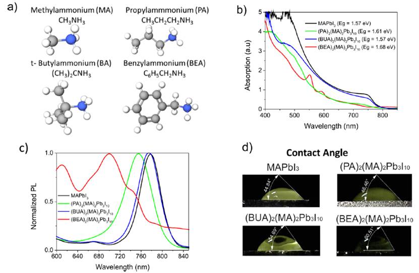
Figure 1 Two-dimensional perovskites. a) Structure of the different organic cations us.ed to synthesize the layered perovskites. b) Absorption spectra and c) PL intensity for the thin films of layered perovskites. d) Photograph of contact angle of water drop indicating superior hydrophobicity for the layered perovskites
The structure of the obtained materials was corroborated by X-ray diffraction (XRD). As shown in Figure 2, the 3D structure of the MAPbI3 perovskite was modified, and hybrid layered perovskites were obtained, as confirmed by the appearance of the new peaks at low diffraction angles. The layered materials corresponded to (PA)2(MA)2Pb3I10, (BUA)2(MA)2Pb3I10, and (BEA)2(MA)2Pb3I10, a product of slicing the 3D perovskite into well-defined 2D slabs.
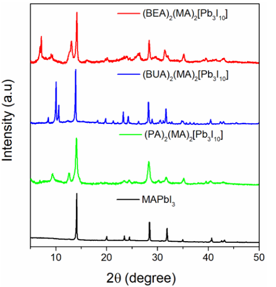
Figure 2 Experimental XRD spectra for three-dimensional perovskite (MAPbI3) and the two-dimensional perovskites
In order to explore the stability in the layered materials, the films were exposed to a moisture stability test at ~80% Relative Humidity. Figure 3a shows the evolution of the films up to 27h exposition time. MAPbI3 sample showed very evident degradation, and after 19h, translucent yellowish zones were formed, indicating perovskite hydration.[26] On the other hand, the layered samples only started to show some important change in color after 27h, and therefore, they were more stable, as shown in Figure 3b. The stability trend followed the previous indications in which more stable films are obtained when a larger cation is introduced.
Temperature stability is also an important aspect for photovoltaic applications since it was previously demonstrated that organic cations such as formamidinium (FA) can improve the thermal stability of the perovskite.[27] [28] Therefore, the films were also exposed to a temperature stability test at 85 °C for 15 days. Like the moisture test, the layered perovskites presented improved thermal stability compared to the 3D MA-based perovskite, probably due to the more difficult volatilization of the large organic cations compared to the MA.
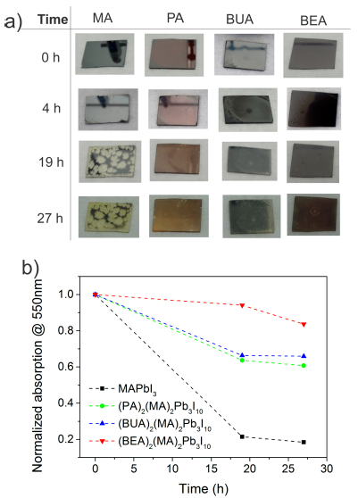
Figure 3 Improved moisture stability of 2D perovskites. a) Images of the films and b) Absorption decay as a function of time for the moisture stability test at 80 % R.H
The introduction of the large inorganic cations in the 2D perovskites had an impact on the morphology of the materials, as observed in Figure 4a. MAPbI3 sample showed a common morphology composed of well-defined grains with an average size of 180 nm. For the (PA)2(MA)2Pb3I10 perovskite with two additional linearly connected carbons, the morphology presented less defined grains embedded in what seems to be an amorphous phase. This phase should correspond to small grains limited in size by the PA layer, which confirms that the layered structure does not have a large-range 3D continuous order. On the other hand, for the case of the BUA cation with three extra carbon atoms in the (BUA)2(MA)2Pb3I10 structure, large grains could be obtained, probably because this branched cation only results in a continuous chain of 2 carbon atoms, making the separation of the layers shorter than for the PA cation, as previously discussed in terms of its smaller unit cell. The phenyl group in the BEA cation is the largest group in the layered perovskites; it allowed the formation of small grains that are smaller than the ones formed by BUA, but larger than those formed by PA cations, probably because of a better interaction between the phenyl groups. This difference in morphology is very important since the transport properties of these materials are remarkably influenced by the phase continuity.[29] Consequently, it would be ideal to have improved moisture and temperature resistance, with less affected transport properties.
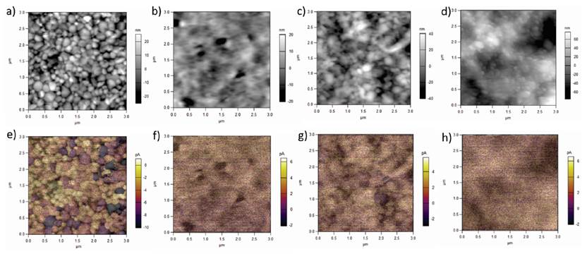
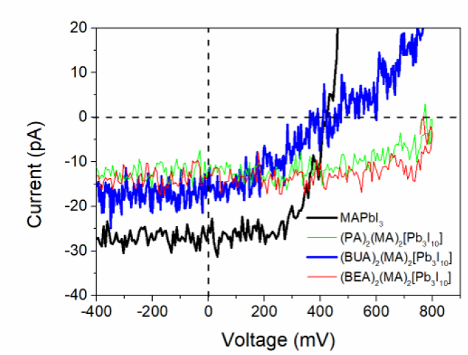
Figure 4 Morphology and electrical properties of layered perovskites. a-d) AFM images showing the morphology of MAPbI3, (PA)2(MA)2Pb3I10, (BUA)2(MA)2Pb3I10, and for (BEA)2(MA)2Pb3I10 films, respectively. e-h) superposed AFM and photoconductive AFM images of MAPbI3, (PA)2(MA)2Pb3I10, (BUA)2(MA)2Pb3I10, and for (BEA)2(MA)2Pb3I10 films, respectively
In order to study both, photoactive and transport properties of the films, photoconductive AFM was performed. The films were illuminated while a voltage sweep between -400mV and 800mV was applied. This allowed obtaining a J-V curve that served to compare the photovoltaic properties of the films, as indicated in Figure 5. The generated current followed the decreasing order, 3D MAPbI3 >BUA- >BEA-> PA-based 2D perovskites, but the Voc increased in the opposite way because of the larger band gaps of the layered perovskites. The photoconductive AFM images were superposed to the morphology images, as shown in Figure 4e-4h. 3D MAPbI3 presented a well-defined contrast between the produced current and each individual grain, similar to reports that suggested transport dependence upon material’s facets[30]. The (BUA)2(MA)2Pb3I10 sample was the only layered perovskite that produced some contrast between grains, indicating the closer behavior to a 3D perovskite.
The high quality and uniformity of the layered perovskite films encouraged the fabrication of planar photovoltaic devices. Solar cells fabricated with these films yielded interesting results compared to the 3D perovskite. Table 1 summarizes the photovoltaic performance of the fabricated devices. The reference device for the MAPbI3 sample resulted in an average power conversion efficiency of 15.02%, with a best performing device of 16.16%. (PA)2(MA)2Pb3I10 and (BEA)2(MA)2Pb3I10 devices presented an average efficiency of 1.10% and 2.19%, respectively. This low performance was mainly determined by the low obtained current. This is an expected result since the relatively poor efficiency in layered systems is due to the inhibition of out-of-plane charge transport by the organic cations, which acts as an insulating spacing layer between the inorganic conduction slabs, and therefore, one approximation to the best results relies on the possibility to have films with a preferential out-of-plane alignment with respect to the contacts to facilitate efficient charge transport[17]. The improved current for the (BUA)2(MA)2Pb3I10 layered perovskite material led to better photovoltaic performance, reaching a 10.35% best and an 8.25% average efficiency, respectively.
Table 1 Summarized photovoltaic parameters of the fabricated devices. Note: values in parenthesis correspond to the parameters of the best-obtained devices
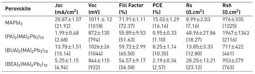
Figure 6a shows the representative J-V curves for all the obtained devices. The EQE shown in Figure 6b corroborated the obtained current, which presented a similar tendency as in the photoconductive AFM in the order, 3D MAPbI3 >BUA- >BEA-> PA-based 2D perovskites. On the other hand, comparative long-term stability measurements for all perovskites were performed in devices without encapsulation exposed to 60% R.H. The efficiency evolution for this test is shown in Figure 6c. A faster decay was observed for the 3D perovskite, resulting in almost null efficiency after 1700 h, while the (PA)2(MA)2Pb3I10 and (BEA)2(MA)2Pb3I10 perovskites showed a slower decay, but due to the low performance, this improved stability did not represent any advantage. On the contrary, (BUA)2(MA)2Pb3I10 retained 68% of its initial value, resulting in devices with an average efficiency of 5.98% after 1700 h.
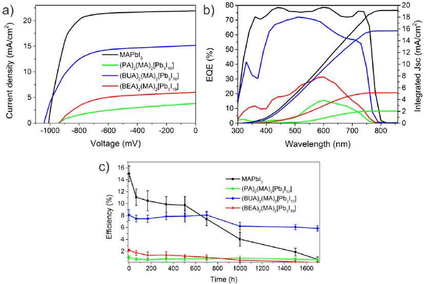
Figure 6 Photovoltaic performance of layered perovskites. a) Representative J-V curves, b) EQE spectra, and c) stability test at 60 % R.H up to 1700h for perovskite devices without encapsulation
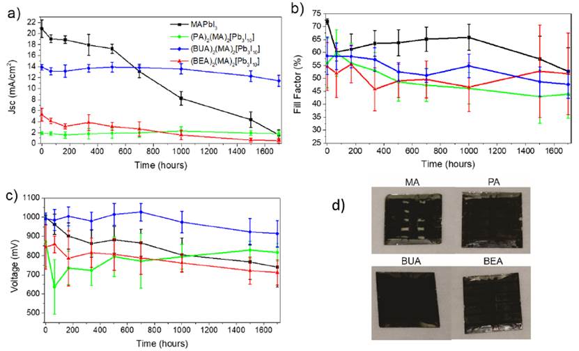
The main factor affecting the efficiency decay was Jsc degradation, as observed in Figure 7a-c for Jsc, Voc, and FF decay. The MAPbI3 devices started to become transparent [Figure 7d), suggesting that the most probable degradation mechanism was perovskite hydration[26], which was less evident for the two-dimensional samples.
4. Conclusions
We have deeply studied different hybrid perovskite materials based on the Ruddlesden-Popper´s family. Structural characterization and device performance demonstrated that the right selection of the organic cations plays an important role in the final perovskite morphology and properties since the three large organic cations used to fabricate the layered perovskites showed improved moisture and thermal stability but marked differences in the photovoltaic performance. Additionally, an efficiency of 10.35% for the devices with (BUA)2(MA)2Pb3I10 used as the active layer was obtained. These unencapsulated devices retained 68% of their performance when exposed to 60% R.H during 1700h, which is superior to the control MAPbI3 devices. Our results indicate that the proper selection of the organic spacer in a two-dimensional perovskite is crucial for achieving better stability of PSCs.

