


 Inglês (pdf)
 Artigo em XML
 Referências do artigo
 Enviar este artigo por email
 Citado por SciELO
  Citado por Google
  Similares em
SciELO
Similares em
SciELO  Similares em Google
 Permalink
1. INTRODUCTION
The need to provide information on the health of people from non-invasive methods is one of the main interests of current medicine. Bioimpedance has proven to be a very useful and safe non-invasive technique [1]. This consists in measuring the conductivity of a biological tissue, which can be characterized by injecting a known current and measuring the resulting voltage at a certain frequency [1], being a good method to detect various types of cancer and measure different physiological variables [2]. One of the main components for the measurement of bioimpedance is the current source, which must have high bandwidth and high output impedance [3]. These current sources are designed from operational amplifiers and feedback loops based on resistive elements and in some cases, in [4] resistive-capacitive. The most popular current sources are the improved Howland [5], the Tietze [6] and the current mirror topologies [7]; considering the source of Howland as having the best performance for bioimpedance measurements [1].
The behavior of these sources should take into account the tolerance of the elements used, the bandwidth and the effect of the parasitic capacitances [3] this leads to the fact that it is difficult to predict the range of frequencies and loads for which a constant effective value current is achieved. Several works have been carried out that attempt to overcome these drawbacks from the analog electronic approach, using different configurations of the Howland source, adding components to the feedback networks as transconductors [7], or including topologies of parallel current sources [8]; but all of them have in common the increase of the analog circuitry. Some papers have opted for the design of integrated circuits tailored for portable systems of bioimpedance measurement, but with limitations in the frequency range in which they work [9]. There are few developments in the area that address the issue from a different approach, either developing specific integrated circuits or using digital systems for signal processing, as was done in [10], where they approach the problem using a voltage source controlled through of an array of programmable logic gates in the field (FPGA), or as in [11], [12], [13] and [14] where the sources used consist of a voltage-to-current converter, which receives signals from a converter digital to analog controlled by an FPGA and in [15] make use of a PSoC 5LP hybrid electronic device to control a signal generator connected to a voltage controlled current source.
As a common element in the previous proposals, it is emphasized that the design of the source does not consist of a single device and the generation of signals is done through an embedded algorithm and a digital-to-analog converter that injects voltage signals directly into the load or through a Howland voltage-to-current converter.
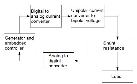
The architecture proposed in this article follows the same line observed in the state of the art, composed of the elements shown in figure 1, where a bipolar sinusoidal voltage source is proposed, with current control, fully embedded in a PSoC 5LP and as the only external element, a resistance of 100 Ω that is placed in series with the load (shunt resistance). The voltage value measured in the shunt resistor allows to know by means of the ohm law, the current that flows towards the load.
2. METHODOLOGY
Bipolar Current Sources
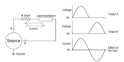
To generate a bipolar sinusoidal current signal on the load, the scheme shown in figure 2 was used, where the load impedance is not referenced to the ground of the source if not connected to two outputs that generate half a positive cycle of a signal sinusoidal with phase shift of 180 degrees, producing circulation of current through the load, from the output that generates the signal to the one that is not doing it.
The PSoC 5LP has the IDAC, which is a digital to analog current converter that works in source mode or sink mode and has a higher sampling frequency than the digital to analog voltage converter. To generate a bipolar current using only IDACS, it is required to connect one to each end of the load. While one IDAC is in source mode, the other must be in sink mode and every half cycle of the signal the current direction must be changed by inverting its working modes. This arrangement generates distortion from the 500 Hz of the output signal, which is why we chose the configuration presented in figure 3 where two IDACs are used in source mode and its output current is transformed into voltage by means of a TIA ( transimpedance amplifier) by its acronym in English).
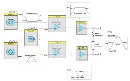
This configuration injects a voltage signal into the load, which controls, by its amplitude, the amplitude of the bipolar current that appears in the load and introduces an element such as the TIA to vary the gain of the output signal. The function of the operational amplifiers in voltage follower mode is to adapt impedance and drive current up to 20 mA. Using the IDACS in the lower current range (0 to 31.875μA) and modifying the value of the TIA feedback resistance, output voltage variations of up to 4.0625 volts can be obtained.
Generation of the Sinusoidal Signal
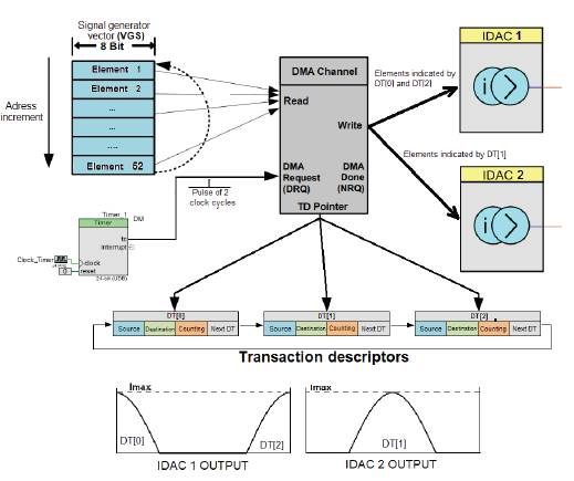
The signal is generated by periodically transferring to the IDACS, through a DMA channel, the elements of a vector of 52 elements, corresponding to the number of samples required to achieve a harmonic distortion of the signal generated close to 1%. The signal generation vector (VGS) is constructed using equation (1), where D [k] is the value of the sample k th, D max is the desired maximum value at the input of the IDAC, N is the number of samples per period and k is an integer that takes values from 0 to N-1.
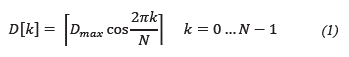
Figure 4 shows the way in which the elements of the signal generation vector (VGS) are distributed, ensuring that each IDAC generates a half cycle of the signal according to the distribution of elements of the vector specified in the descriptors of the transaction DMA (DT [0], DT [1], DT [2]). The final signal is achieved through the periodic and sequential execution of the descriptors of the DMA transaction.
Measurement of the Current Signal
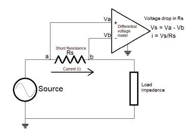
The measurement of the current is done indirectly, measuring the voltage at a resistance of 100 Q, which is in series with the load impedance as seen in figure 5. The meter is a high input impedance element, which measures the difference in voltage between points a and b relative to the ground of the source. Through the ohm law, the current value that flows through the shunt resistance and the load is obtained.
The analog to digital converters of the PSoC have a much lower sampling frequency than the IDACs, for this reason, it is not possible to carry out a fine control of the amplitude and shape of the sinusoidal output current, which is why the control approach adopted was minimalist regarding the use of hardware resources. A configuration that controls the peak amplitude of the current signal was chosen, reading the voltage at the shunt resistance at the instant when the output signal has maximum amplitude.
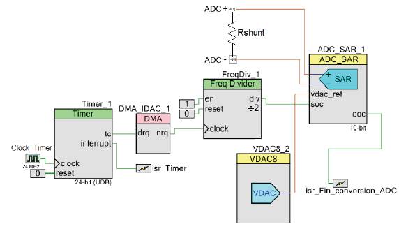
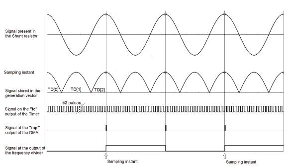
Figure 6 shows the configuration for the measurement of the current that was implemented in the PSoC; here an analog and digital converter of successive approximations (SAR) in differential mode is used, sampling frequency of 1.125 Mps and 10-bit resolution which uses an end-of-conversion interruption to deliver the measured voltage between the terminals of the derivation resistance, to the control algorithm. The DMA module was configured so that at the end of the transfer of the VGS vector, it was sent to the SAR up to the pulse of the time cycles of duration, in order to start the analog and digital conversion. According to the SAR, such a narrow pulse has not been detected, a frequency divider has been used to increase the width of the trigger pulse, an amplitude control must be carried out, peak current, each of the periods of the generated signal, see figure 7. The function The VDAC is the maintenance of a voltage of 0.8 volts to SAR.
Source: author's own elaboration.
FIGURE 6 CURRENT MEASUREMENT WITH SHUNT RESISTANCE IMPLEMENTED IN PSOC
Control Scheme
Varying the amplitude of the output signal is possible by multiplying each sample of the VGS vector by a scale factor, or by using different generation vectors and choosing the most convenient one for the desired amplitude. The first option was discarded for having a high processing time, in the second option the configuration presented in figure 8 was used, where we have an array of unsigned 8-bit integers of size 196x52, with all the possible generation vectors of the signal (MPVG). Each row of the matrix MPVG corresponds to a generation vector created from equation (1). Row 0 of the MPGV matrix corresponds to the samples for a Dmax of 60, row 1 for a Dmax of 61, and so on up to a Dmax of 255; Dmax values less than 60 were not considered because they produced amplitude distortion in the output signal, due to the use of few quantization steps in the digital to analog converter.
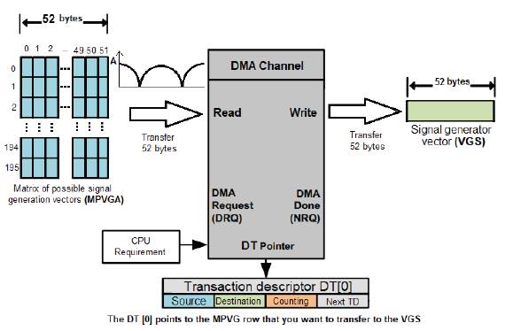
Each time the controller requires an amplitude change in the output signal, it can modify the feedback resistances (Rfb) of the TIA, see figure 3 and / or update the vector VGS with the appropriate vector contained in any row of the matrix MPVG. This update is done by the CPU, making a software request to a DMA channel destined for this purpose see figure 8.
Controller
The control scheme is shown in figure 9, here the input to the controller is the factor e[k], which is the quotient between the reference and the differential voltage value measured at the terminals of the shunt resistor at the time of sampling k-th. The controller affects the plant by means of V[k], which is the peak voltage level of the output signal. The plant consists of a shunt resistance of 100 Q, which is in series with the load impedance. By Ohm's law we can know the peak current flowing to the load, by measuring the peak voltage amplitude in the shunt resistor. Equations (2) to (6) describe the behavior of the controller, which is composed of software and hardware components.
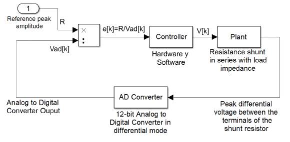
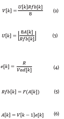
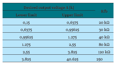
Where V(k) is the peak voltage value at the output of the source, U(k) is an 8-bit unsigned integer that takes values between 60 and 255 and represents the peak amplitude of the signal generation vector, which is chosen from the matrix of possible sample vectors of the signal and updated by a DMA transfer, see figure 8, Rfb(k) is the feedback resistance of the transimpedance amplifiers, chosen by a function F described in table 1, e[k] is the quotient between the reference and the peak voltage measured at the shunt resistance, R is the desired peak reference voltage value at the shunt resistance at the sampling instant k, Vad is the peak voltage value measured by the analog to digital converter between the terminals of the shunt resistor. Equation 6 shows the central core of the controller, here A(k), which is the peak voltage value to which the output of the source is to be taken, before being bounded by the hardware conditions stated in equations 2 to 5.
3. RESULTS AND DISCUSSION
In this section the experimental results obtained with the proposed source are presented; performing three types of tests: (i) current versus load impedance, using a Cole circuit, (ii) current versus frequency using resistive loads and (iii) total harmonic versus charge distortion for a constant frequency. The current injected into the load is calculated by measuring the voltage in the shunt resistor, with a value of 100 Ω, using a digital oscilloscope (Tektronix TBS 1052B).
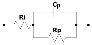
Current Versus Load Impedance for a COLE Circuit
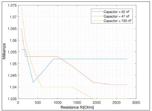
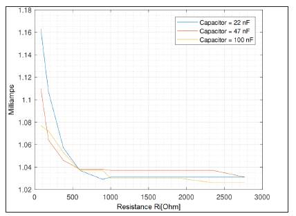
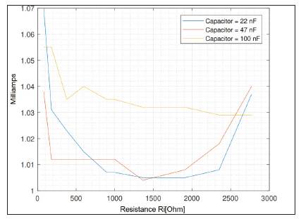
Figures 11, 12 and 13 show the amplitude of the current as a function of the resistance Ri and the capacitance Cp of the cole model shown in figure 10. The frequencies considered are 1 kHz, 50 kHz and 120 kHz. Rp has a constant value of 180 Ω and in all the figures the resistance R takes the following values: 81 Ω, 181 Ω, 378 Q, 596 Ω, 896 Ω, 1000 Ω, 1364 Ω, 1908 Ω, 2350 Ω, and 2770 Ω.
Source: author's own elaboration.
FIGURE 11 PEAK CURRENT AMPLITUDE OVER A LOAD IMPEDANCE TYPE COLE, VARYING THE RESISTANCE RI AND THE CAPACITANCE CP, FOR A FREQUENCY OF 1KHZ AND REFERENCE CURRENT OF 1MA
Source: author's own elaboration.
FIGURE 12 PEAK CURRENT AMPLITUDE OVER A LOAD IMPEDANCE TYPE COLE, VARYING THE RESISTANCE RI AND THE CAPACITANCE CP, FOR A FREQUENCY OF 50KHZ AND REFERENCE CURRENT OF 1MA
Current Versus Frequency
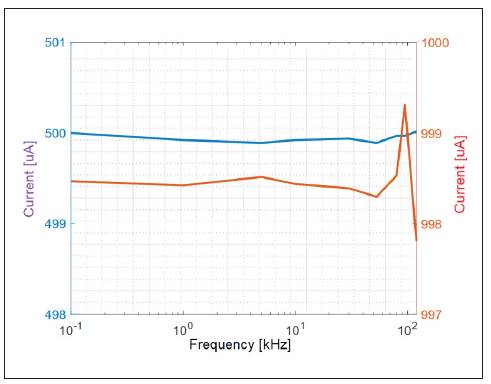
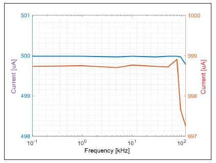
Figures 14 and 15 show the peak amplitude of the current delivered to a pure resistive load as a function of frequency. A load of 1000 Ω and 3100 Ω was used. In the two graphs, the frequency values used are 0.1 kHz, 1 kHz, 5 kHz, 10 kHz, 30 kHz, 53 kHz, 80 kHz, 95 kHz and 120 kHz.
Source: author's own elaboration.
FIGURE 14 PEAK CURRENT VERSUS FREQUENCY, FOR A LOAD OF 1000 Q. IN BLUE THE CURVE FOR A REFERENCE OF 500 MA AND IN RED FOR A REFERENCE OF 1000 MA
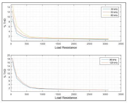
Harmonic Distortion Versus Load Resistance
The total harmonic distortion of the applied current in the load was calculated using the thd function of Matlab. The samples of the current were obtained by measuring the voltage present in the terminals of the shunt resistance and applying Ohm's law. A digital oscilloscope (Tektronix TBS 1052B) was used to perform the voltage measurements.
Figure 16 shows the harmonic distortion for a peak current of 1mA, for frequencies between 30 kHz and 120 kHz.
Discussion of the results
The current source presented in this article uses feedback control to maintain the peak amplitude of the current applied to a load of unknown value. The design combines software elements, represented by equation 6 and hardware elements such as IDACs, TIA transimpedance amplifiers, VDACs and voltage trackers, represented in equations 2 to 5, all these elements embedded in a single mixed signal device PSoC 5LP CY8C5888AXI -LP096.
It can be seen in figures 11 to 15 that for load resistance values higher than 500 Q, the deviation of the peak current value of the output signal with respect to the reference does not exceed 5% and the frequency variations with respect to a fixed load, maintain current values practically constant and very close to the established reference, which suggests that the architecture proposed in figure 1 is valid for the construction of current sources in the context of bioimpedance. In practice, the convergence of the peak output current with respect to the reference is limited by the precision with which the peak output voltage of the source is generated. The difference between the desired value and the real value is caused by the quantization of the two IDACs and the digital analog converter that reads the voltage in the shunt resistor; another source of error is the limited number of feedback resistances of the TIA see table 1.
For low values of load resistance, the harmonic distortion increases, since, in order to maintain a constant current value, the source is required to generate small peak voltage values, forcing it to generate the output signal with few quantization steps, which It results in distortion in the form of the generated sinusoidal signal.
The maximum frequency generated by the device is limited by the maximum sampling frequency of the IDACs (8 MHz) and the maximum transfer rate of the DMA channel (6 MHz). In the proposed design, the transmission of the 52 samples of the VGS vector via a DMA channel to the IDACs limits the frequency of the output signal to 125 kHz. However, it is important to clarify that this limitation is not inherent to the proposed design, but to the hardware limitations of the device used for the implementation.
The control of the peak amplitude of the signal converts the problem of current control in the monitoring of a fixed reference every period of the output signal, maintaining an acceptable harmonic distortion if the generation of the signal is avoided using few quantization steps; it was shown that a simple controller that multiplies the current voltage output by the quotient between the immediately preceding output and the reference, see equation 6, is more than enough to maintain the peak amplitude of the signal close to the desired one. The update of the vector of generation of the signal by a new one by DMA transfer, each time the controller requires adjustments in the level of the output signal, allows the controllability of the current without direct intervention of the CPU and ostensibly increases the capacity of the device to generate higher output frequencies.
The maximum load value that the source can handle is limited by the maximum output voltage produced by the circuits proposed in figure 3, which is equal to 4.0625 V and also by the peak current that it is desired to inject into the load.
4. CONCLUSION
A current source has been proposed for bioimpedance studies with an architecture totally embedded in a mixed signal device. The control of the current is based on a discrete time non-linear algorithm that guarantees the convergence of the measured current to its desired value. The algorithm does not require any parameter adjustment. The proposed approach obtains low differences between the desired current and the measurement for frequencies close to the maximum frequency at which the IDACs can operate. Future work will be devoted to improving the non-linear algorithm to control both the amplitude and phase of the current in the load, as well as the increase in the frequency of the source output.

