


Services on Demand
Journal
Article
 English (pdf)
 Article in xml format
 Article references
 Send this article by e-mail
Indicators
-
 Cited by SciELO
 -
 Access statistics
Related links
-
 Cited by Google
 -
 Similars in
SciELO
Similars in
SciELO -
 Similars in Google
Share

 Permalink
Universitas Scientiarum
Print version ISSN 0122-7483
Univ. Sci. vol.19 no.2 Bogotá May/Aug. 2014
Hall effect and transient surface photovoltage (SPV) study of Cu3BiS3 thin films
Efecto Hall y estudio de fotovoltaje superficial transiente (SPV) en películas delgadas de Cu3BiS3
Efeito Hall e estudo de foto voltagem superficial transiente (SPV) em películas delgadas de Cu3BiS3
F. Mesa1, A. Dussan2, B. A. Paez-Sierra3, H. Rodriguez-Hernandez3
Edited by Beynor Paez & Alberto Acosta
1Unidad de Estudios Universitarios, Universidad del Rosario, Bogotá, Colombia.
2Departamento de Física, Grupo de Materiales Nanoestructurados, Universidad Nacional de Colombia - Bogotá, Colombia.
3Thin films and Nanophotonics Group, Pontificia Universidad Javeriana, Bogotá, Colombia.
Funding: Pontificia Universidad Javeriana; Banco de la República; Fundación para la Promoción de la Investigación y la Tecnología (FPIT).
Electronic supplementary material: N/A
Received: 22-11-2013 Accepted: 25-03-2014 Published on line: 10-04-2014
Para citar este artículo / To cite this article
Mesa F, Dussan A, Paez-Sierra BA, Rodriguez-Hernandez H (2014) Hall effect and transient surface photovoltage (SPV) study of Cu3BiS3 thin films. Universitas Scientiarum 19(2): 99-105 doi: 10.11144/Javeriana.SC19-2.ehef
Abstract
Here, we present the electrical properties of the compound Cu3BiS3 deposited by co-evaporation. This new compound may have the properties necessary to be used as an absorbent layer in solar cells. The samples were characterized by Hall effect and transient surface photovoltage (SPV) measurements. Using Hall effect measurements, we found that the concentration of n charge carriers is in the order of 1016 cm3 irrespective of the Cu/Bi mass ratio. We also found that the mobility of this compound (μ in the order of 4 cm2 V-1s-1) varies according to the transport mechanisms that govern it and are dependent on temperature. Based on the SPV, we found a high density of surface defects, which can be passivated by superimposing a buffer layer over the Cu3BiS3 compound.
Keywords: Electric transport; Cu3BiS3; transient surface photovoltage; defects.
Resumen
Se presentan las propiedades eléctricas del compuesto Cu3BiS3 depositado por co-evaporación. Este es un nuevo compuesto que puede tener propiedades adecuadas para ser utilizado como capa absorbente en celdas solares. Las muestras fueron caracterizadas a través de medidas de efecto Hall y fotovoltaje superficial transiente (SPV). A través de medidas de efecto Hall se encontró que la concentración de portadores de carga n es del orden de 1016 cm-3 independiente de la relación de masas de Cu/Bi. También se encontró que la movilidad de este compuesto (μ del orden de 4 cm2V -1s-1) varía de acuerdo con los mecanismos de transporte que la gobiernan en dependencia con la temperatura. A partir de las medidas de SPV se encontró alta densidad de defectos superficiales, defectos que son pasivados al superponer una capa buffer sobre el compuesto Cu3BiS3.
Palabras clave: Transporte eléctrico; Cu3BiS3; fotovoltaje superficial transiente; defectos.
Resumo
Apresentam-se as propriedades elétricas do composto Cu3BiS3 depositado por co-evaporação. É um composto novo que pode ter as propriedades adequadas para ser utilizado como capa absorvente em células solares. As amostras foram caracterizadas através de medidas do efeito Hall e foto voltagem superficial transiente (SPV). Através de medidas do efeito Hall se encontro que a concentração de portadores de carga n é da ordem de 1016 cm3 independentemente da relação de massas de Cu/Bi. Também se encontrou que a mobilidade des composto (μ da ordem de 4 cm2V -1s-1) varia de acordo com os mecanismos de transporte que a governam em dependência com a temperatura. Partindo das medidas de SPV se encontrou uma alta densidade de defeitos superficiais, defeitos que são passivados a sobrepor uma capa buffer sobre o composto Cu3BiS3.
Palavras-chave: Transporte elétrico; Cu3BiS3; foto voltagem superficial transiente; defeitos.
Introduction
I-III-VI2 chalcopyrite compounds are direct gap semiconductors and have adequate properties for use in the fabrication of single-junction cells or tandem cells (Repins et al. 2008, Kayes et al. 2011, Choi et al. 2012, Seo et al. 2012). Nevertheless, the maximum conversion efficiency reported up to date for single-junction thin film technology solar cells was obtained by fabricating the device using Cu-III-VI2 group compounds as the absorbing layer (Contreras et al. 2009, Green et al. 2012). These solar modules which are based on a thin film of Cu (InGa)Se2 (CIGS) offer greater stability and price competitiveness for production processes. By contrast, Cu-V-VI2 based compounds are characterized by having a forbidden bandgap that varies between values from 1.15 to 2.73 eV, which makes this kind of compounds potentially useful and attractive candidates for photovoltaic applications (Bar et al. 2008, Kawamura et al. 2009, Meiss et al. 2011, Mõmg et al. 2011, Tadjarodi et al. 2012).
For these reasons, Cu3BiS3 compound has taken great importance in optoelectronic applications. This compound grows in a "wittichenite" type orthorhombic crystalline lattice, where this phase is obtained at 300°C temperatures (Naiding 1994, Razmara et al. 1997). Several techniques have been used for the preparation of Cu3BiS3 samples, such as evaporation (Mesa et al. 2009, Colombara et al. 2012), via PEG (polyethylene glycol) (Yan et al. 2012), reactive sputtering (Gerein et al. 2006), and CBD (Chemical Bath Deposition) (Estrella et al. 2003). Nevertheless, it is reported that with the use of CBD there is growth of a metallic Bi thin film which is deposited by thermal evaporation on CuS obtained by CBD. As a result of this study the layers presented p-type conductivity (∼0.03 Ω-1cm-1) and an energy gap Eg- of 1.28 eV These are photoconductive, and the product of the mobility by the life time of the photo-generated carriers is ∼10-6 cm2V-1. In work carried out by N. Gerein and J. Haber (Gerein et al. 2006 a,b) it is reported that layers deposited by reactive sputtering in one or two phases, and then annealed in an H2S atmosphere present electrical resistivities in the range between 3-200 Ωcm, a forbidden band gap (Eg) of 1.4 eV and an absorption coefficient of 1x105 cm-1.
In the present work, Cu3BiS3 samples were deposited by evaporation processes, varying the mass ratios mCu/(mCu+mBi). Emphasis was made on studying the effect of the Cu/Bi ratio on the concentration of mobile charge carriers. From transient surface photovoltage (SPV) measurements, the effect of the addition of a buffer layer on the compound was also observed.
Materials and Methods
Samples of Cu3BiS3 were deposited by the method of evaporation of precursors varying the mass ratios mCu/(mCu+mBi) between 0.43 to 0.49. Additionally, Hall voltage measurements were carried out on Cu3BiS3 samples, using Al as electrical contact. The Hall voltage measurement system is composed of:
Chamber with prevacuum system, sample heating and cooling system, and Hall voltage measurement system, which in turn is composed of model 7065 Hall effect card and a Keithley model 7001 Switch System. The Hall voltage measurement system is described in detail in the reference (Gutiérrez et al. 2007). The concentration of mobile charge carriers is calculated from the Hall voltage measurements by following an experimental procedure developed by the Keithley firm, which is based on the Van der Pauw method and the ASTM (American Society for Testing and Materials 1991) F 76 standard.
Surface photovoltage (SPV) measurements were taken using a capacitor composed of a Cr semitransparent electrode (transparency around 70% and diameter d=5mm) evaporated on a quartz crystal; a mica (width d=50μm) as dielectric and the sample deposited over a conducting substrate (reference electrode). The photovoltage signal is recorded through a lock-in amplifier taking the drop in voltage over the charge resistance R. A pulsated laser NT343/1/UVE (EKSPLA) was used, where the pulse duration was around 5 ns and a maximum intensity of 0.5 mJ/cm2 (Fu et al. 2014).
Results
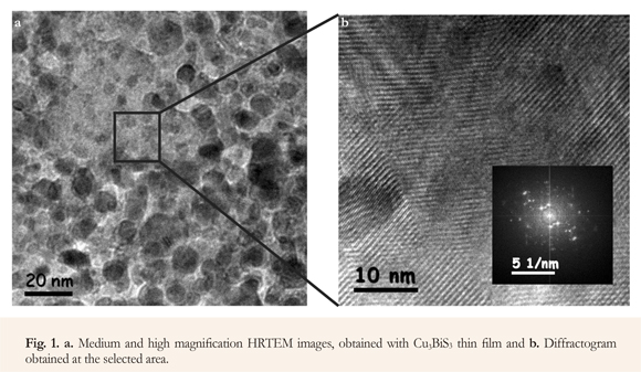
HRTEM images of medium and high magnification measured in a specific area of Cu3BiS3 thin films, show that this compound grows in a nanocrystalline lattice, with grains of different size, whose average value is in the vicinity of 15 nm (Mesa et al. 2012). On the other hand, due to the nanocrystalline feature of the samples, it is hard to perform the corresponding indexation. Nevertheless, the diffraction pattern of the selected area is shown in the image (Figure 1).
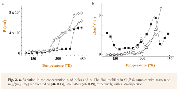
With the aim of deepening in the study of electrical transport properties of Cu3BiS3 thin films, the p concentration and the μ mobility of charge carriers was determined from measurements of electrical conductivity and Hall coefficient as a function of temperature. The p vs T and μ vs T curves for Cu3BiS3 thin films deposited with varying mCu/(mCu+mBi) ratio are analyzed (Figure 2).
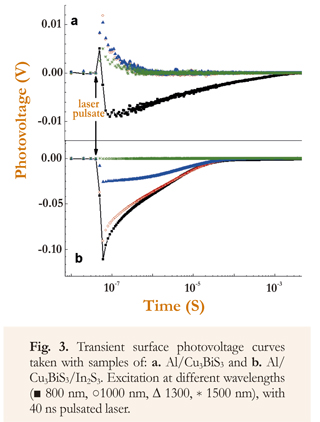
Additionally, transient SPV curves were obtained with Cu3BiS3 thin films and with Cu3BiS3/In2S3 system, using photoexcitation at different wavelengths (Figure 3). From these results it is observed that the transient SPV signal, obtained with Cu3BiS3 films excited with wavelengths greater than the gap (<890 nm) is positive, with a decay time constant of ∼0.1 μs. Nevertheless, when the sample is excited with wavelengths smaller than the energy gap (<890 nm), the SPV signal decay has negative values.
Discussion
The results show that a significant increase in the p concentration of carriers is observed at temperatures greater than 250 °K, apparently caused by thermal excitation of electrons from extended states at the valence band toward accepting states within the gap, thus generating an increase in the density of negatively ionized accepting impurities (Figure 2). The results also show that the sharp increase in the conductivity of Cu3BiS3 thin films observed at temperatures greater than 250 °K (Mesa et al. 2009), is basically caused by an increase in the concentration of carriers at this range of temperatures (Kehoe et al. 2013).
It is also observed that the Cu3BiS3 samples present low mobility, probably due to the fact that the samples deposited by co-evaporation present a high density of native defects and ionized impurities affecting mobility (Figure 2). Also, it is observed that by increasing temperature, mobility increases, and the increase is sharp at temperatures greater than 250 °K (especially in samples with a mass ratio of 0.46 and 0.49). This behavior might be explained by assuming that when temperature increases a greater quantity of carriers are excited from states at band tails towards states in a valence band region with lower effective mass (they become lighter). Nevertheless, it may also be observed that when temperature increases, carriers in grain boundary states are excited into the valence band, inducing thus a decrease in the height of the grain boundary barrier Ob. On the other hand, the mobility of the sample with mass ratio of 0.43 presents a different behavior at the low temperature region (T<150 °K), which may be caused by a decrease in the probability that the carriers are displaced from a localized state into another via tunnel, in turn caused by some unknown mechanism.
Nevertheless, this disordered nanocrystalline feature of Cu3BiS3 films (Figure 1), causes the formation of a high density of associated states and point defects and incomplete bonds with high density grain boundaries, which are responsible for the low mobility values measured in this kind of samples, and for the formation of localized states allowing electrical transport via hopping.
From these results it is established that the generation of positive surface photovoltage when the Cu3BiS3 film is excited with photons of wavelength λ>890 nm (Figure 3), occurs because in this case the excitation of electrons is induced from surface states towards the conduction band, which causes a decrease in the deflection of bands in the surface region, which in turn causes an increase in the SPV value. When the excitation is done with photons of wavelength λ<890 nm, there is simultaneously an excitation of electrons from surface states to conduction bands, which causes positive SPV values, and fundamental excitation (transition of electrons from valence band to conduction band), which are diffused into surface states, giving rise to negative SPV values. As the negative effect of the fundamental electron transition is dominant, the net SPV value turns out to be negative (Mesa et al. 2010).
Moreover, it is observed that the transient SPV curves obtained with Cu3BiS3/In2S3 samples do not present change of sign and their values are generally negative, except in the case in which the excitation is done with very low energy photons (λ=1500 nm), where the SPV change is not present (Figure 3). In this case, wavelengths longer than the In2S3 gap were chosen (λG=688 nm), in order to avoid excitation of electrons through fundamental absorption.
From obtained results it is observed that negative transient SPV of Cu3BiS3/In2S3 system decays further (two orders of magnitude), in comparison with the Cu3BiS3 negative transient SPV, apparently due to the passivation of Cu3BiS3 surface states, which causes elimination of the positive contribution in the SPV net value (Figure 3). Also, it is observed that the SPV value decreases as the excitation wavelength increases; this behavior is due to the fact that the decrease in energy from photons with the increase in λ, causes a decrease in the density of electrons photogenerated in the Cu3BiS3, which move (by diffusion and drag) toward surface states of the In2S3, thus reducing the net measured value of transient SPV. Measurements carried out with 1500 nm excitation show that there is no change in the SPV signal, indicating that the energy of the photons is lower than the activation energy of Cu3BiS3 and In2S3 surface states.
The experimental results presented here lead to the following interpretations. The Cu3BiS3 thin film surface presents a high density of surface states, where the emitted electrons are conducted to the surface generating a positive SPV value. These states are distributed within the Eg, indicated by the start of the SPV at approximately 0.5 eV The best distribution range for this work function agrees with that.
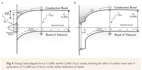
The energy band diagrams for Cu3BiS3 and for Cu3BiS3/In2S3 system show both the effect of the surface states on the surface deflection of the bands (Figure 4), causing the surface photovoltage changes observed in Cu3BiS3 films, and the effect of Cu3BiS3 surface state passivation on Cu3BiS3/In2S3 system surface photovoltage, which takes place when the In2S3 layer is deposited on it.
Conclusion
The Cu3BiS3 samples were grown by evaporation. From Hall effect and transient surface photovoltage measurements, it was found that the disordered nanocrystalline feature of the samples causes the formation of a high density of states associated with point defects and incomplete bonds with a high density of grain boundaries, which are responsible for the low mobility values, causing the formation of localized states which allow electrical transport via hopping. Nevertheless, when a buffer layer of In2S3 is included on the Cu3BiS3 surface, there is a passivation of defect states, improving the quality of the material.
Acknowledgements
This work is supported by several projects from Universidad del Rosario. Special thanks also go to Universidad Nacional de Colombia, QUBITeXp International Trade SAS, Colombia. OFI at Pontificia Universidad Javeriana, projects 4513 and 4515, Banco de la República with Fundación para la Promoción de la Investigación y la Tecnología (FPIT), Project 2954 "Construcción de prototipo de pantalla plana tipo OLED con resolución 200X200".
Conflict of Interest
This work does not present any conflicts of interest.
Referencias
American Society for Testing and Materials (1991) Annual Book of ASTM Standards 10.05. [ Links ]
Bar M, Weinhardt L, Pookpanratana S, Heske C, Nishiwaki S et al. (2008) Band gap energy of chalcopyrite thin film solar cell absorbers determined by soft x-ray emission and absorption spectroscopy. Photovoltaic Specialists Conference, 2008 PVSC '08. 33rd IEEE:1-4 doi: 10.1109/PVSC.2008.4922728. [ Links ]
Colombara D, Peter LM, Hutchings K, Rogers KD, Schafer S et al. (2012) Formation of Qi3BiS3 thin films via sulfurization of Bi-Cu metal precursors. Thin Solid Films 520(16):5165-5171 http://dx.doi.org/10.1016/).tsf.2012.04.003. [ Links ]
Contreras M, Egaas B, Ramanathan R, HiltnerJ, Awarzlander A et al. (2009) "Progress toward 20% efficiency in Cu (In,Ga)Se2 polycrystalline thin-film solar cells". Progress in Photovoltaics: Research and Applications 7:311-316. [ Links ]
Choi IH, Choi CH, Lee JW (2012) Deep centers in a CuInGaSe2/CdS/ZnO: B solar cell. Physica Status Solidi A 209:1192-1197 doi: 10.1002/pssa.201127596. [ Links ]
Estrella V, Nair MT, Nair PK (2003) Semiconducting Cu3BiS3 thin films formed by the solid-state reaction of CuS and bismuth thin films. Semiconductor Science and Technology 18:190-194 doi:10.1088/0268-1242/18/2/322. [ Links ]
Fu Y, Rada T, Fischer CH, Lux-Steiner MCh, Dittrich T (2014) Surface photovoltage spectroscopy on Cu (In,Ga)(S,Se)2/ZnS-nanodot/In2S3 systems. Progress in Photovoltaics: Research and Applications 22:44-50 doi: 10.1002/pip.2305. [ Links ]
Gerein N, Haber J (2006) One-Step Synthesis and Optical and Electrical Properties of Thin Film Cu3BiS3 for Use as a Solar Absorber in Photovoltaic Devices. Chemestry of Materials 18:6297-6302 doi: 10.1021/cm061453r. [ Links ]
Gerein N, Haber J (2006) Synthesis of Cu3BiS3 Thin Films by Heating Metal and Metal Sulfide Precursor Films under Hydrogen Sulfide. Chemestry of Materials 18:62896396 doi: 10.1021/cm061452z. [ Links ]
Green MA, Emery K, Hishikawa Y, Warta W Dunlop ED (2012) Solar cell efficiency tables (version 40). Progress in Photovoltaics: Research and Applications 20:606-614 doi: 10.1002/pip.2267. [ Links ]
Gutiérrez D, Villada A, Tirado L, Codoy H, Cordoba M et al. (2007) Determinación de concentración de portadores y altura de la barrera schottky en películas semiconductoras del sistema GaInAsSb. Revista Colombiana de Física 39(1):147-150. [ Links ]
Kayes BM, Hui N, Twist R, Spruytte SG, Reinhardt F et al. (2011) 27.6% Conversion efficiency, a new record for single-junction solar cells under 1 sun illumination. Higashi: presented at 37th IEEE Photovoltaic Specialists Conference, 2011 doi: 10.1109/PVSC.2011.6185831. [ Links ]
Kawamura M, Fujita T, Yamada A, Konagai M (2009) CIGS thin-film solar cells grown with cracked selenium. Journal of Crystal Growth 311(3):753 doi: 10.1016/j.jcrysgro.2008.09.091. [ Links ]
Kehoe AB et al. (2013) Cu3MCh3 (M = Sb, Bi; Ch = S, Se) as candidate solar cell absorbers: insights from theory. Physical Chemistry Chemical Physics 15:15477-15484 doi: 10.1039/c3cp52482e. [ Links ]
Meiss J, Menke T, Leo K, Uhrich C, Gnehr WM, Sonntag S et al. (2011) Highly efficient semitransparent tandem organic solar cells with complementary absorber materials. Applied Physics Letters 99:043301 http://dx.doi.org/10.1063/1.3610551. [ Links ]
Mesa F, Dussan A, Gordillo G (2009) Evidence of trapping levels and photoelectric properties of Cu3BiS3 thin films. Physica B: Condensed Matter 404:5227-5230 http://dx.doi.org/10.1016/j.physb.2009.08.302. [ Links ]
Mesa F, Gordillo G (2009) Effect of preparation conditions on the properties of Cu3BiS3 thin films grown by a two-step process. Journal of Physics Conference Series 167(1):012019 doi:10.1088/1742-6596/167/1/012019. [ Links ]
Mesa F, Dussan A, Gordillo G (2010) Study of the growth process and optoelectrical properties of nanocrystalline Cu3BiS3 thin films. Physica Status Solidi C 7:917-920 doi: 10.1002/pssc.200982860. [ Links ]
Mesa F, Gordillo G, Dittrich T, Ellmer K, Baier R et al. (2010) Transient surface photovoltage of p-type Cu3BiS3. Appl. Phys. Lett. 96:082113 http://dx.doi.org/10.1063/1.3334728. [ Links ]
Mesa F, Dussan A, Sandino J, Lichte H (2012) Characterization of Al/ Cu3BiS3/buffer/ZnO solar cells structure by TEM. Journal of Nanoparticle Research 14:1054 doi: 10.1007/s11051-012-1054-7. [ Links ]
Mónig H, Kaufmann CA, Fischer CH, Grimm A, Caballero R et al. (2011) Gallium gradients in chalcopyrite thin films: Depth profile analyses of films grown at different temperatures. Journal of Applied Physics 110:093509. [ Links ]
Naiding W (1994) The Cu-Bi-S system: results from low temperature experiments. MineralogicalMagazine 58:201-204. [ Links ]
Razmara MF, Henderson CM, Patrick R et al. (1997) The cristalchemestry of the solid solution series between chalcostibite (CuSbS2) and emplectite (CuBiS2). Mineralogical Magazine 61:79-88. [ Links ]
Repins I, Contreras MA, Egaas B, DeHart C, Scharf J et al. (2008) 19.9%-efficient ZnO/CdS/CuInGaSe2 solar cell with 81.2% fill factor. Progress in Photovoltaics: Research and Applications 16:235-239 doi: 10.1002/pip.822. [ Links ]
Seo JH, Kim DH, Kwon SH, Song M, Choi MS et al. (2012) High Efficiency Inorganic/Organic Hybrid Tandem Solar Cells. Advanced Materials 24:4523-4527 doi: 10.1002/adma.201201419. [ Links ]
Tadjarodi A, Cheshmekhavar AH, Imani M (2012) Preparation of AgInS2 microwave heating technique; study of effective parameters, optical and photovoltaic characteristics. Applied Surface Science 15:449-456 http://dx.doi.org/10.1016/j.apsusc.2012.09.080. [ Links ]
Yan J, YuJuan Z, Wenjun L, Yanan Y, Xiaoyun L et al. (2012) Synthesis of Cu3BiS3 and AgBiS2 crystallites with controlled morphology using hypocrellin template and their catalytic role in the polymerization of alkylsilane. Journal of Materials Science 47:4159-4166 doi: 10.1007/ s10853-012-6270-0. [ Links ]
