


Services on Demand
Journal
Article
 English (pdf)
 Article in xml format
 Article references
 Send this article by e-mail
Indicators
-
 Cited by SciELO
 -
 Access statistics
Related links
-
 Cited by Google
 -
 Similars in
SciELO
Similars in
SciELO -
 Similars in Google
Share

 Permalink
Ingeniería y competitividad
Print version ISSN 0123-3033
Ing. compet. vol.15 no.2 Cali July/Dec. 2013
A methodological approach for asynchronous implementation of the Rijndael Algorithm
Aproximación metodológica para la implementación asíncrona del algoritmo de Rijndael
Rubén D. Nieto
Grupo de Investigación de Arquitecturas Digitales y Microelectronica, Escuela de Ingeniería Eléctrica y Electrónica, Universidad del Valle. Cali-Colombia
E-mail: ruben.nieto@correounivalle.edu.co
Álvaro Bernal
Grupo de Investigación de Arquitecturas Digitales y Microelectronica, Escuela de Ingeniería Eléctrica y Electrónica, Universidad del Valle. Cali-Colombia
E-mail: alvaro.bernal@correounivalle.edu.co
Eje temático: Electrical and electronic engineering / Ingenieria eléctrica y electrónica
Recibido: 23 de Abril de 2013
Aceptado: 26 de Agosto de 2013
Abstract
This article describes the implementation methodology of Rijndael algorithm to encryption process, by using asynchronous design with assistance of the software tool Balsa, for functional simulation, description and synthesis of asynchronous digital circuits. The main results presented correspond to implementations that use the codification protocols dual-rail and 1-of-4, for blocks of data and keys of 128 bits over a field-programmable gate array (FPGA) hardware platform. The Xilinx ISE tool was used showing a full integration level with the Balsa system.
Keywords: Asynchronous, Balsa, FPGA, Rijndael.
Resumen
En este artículo se describe una metodología de implementación del algoritmo de Rijndael para el proceso de encriptación. Se utilizó el estilo de diseño asíncrono con la ayuda de una herramienta conocida como Balsa, la cual permite simulación funcional, descripción y síntesis de circuitos digitales asíncronos. Los resultados obtenidos corresponden a implementaciones que utilizan los protocolos de codificación dual-rail y 1-of-4, para bloques de datos y claves de 128 bits sobre una plataforma hardware de un arreglo de compuertas reprogrammable por el usuario (FPGA). Para la síntesis automática sobre la FPGA se utilizó la herramienta Xilinx ISE, que muestra un completo nivel de integración con el sistema Balsa.
Palabras clave: Asynchronous, Balsa, FPGA, Rijndael.
1. Introduction
In October of 2000, the National Institute of Standards and Technology (NIST) (NIST, 2000), selected the Rijndael Algorithm as the new Advanced Encryption Standard (AES). NIST registered the algorithm as the standard FIPS-197 (Federal Information Processing Standard- document 197) (FIPS, 2001). The Rijndael Algorithm implementations have been done in software and Field Programmable Gate Arrays (FPGAs). Software implementation allows flexibility and low cost, whereas hardware implementation results in better performance. The algorithm has been also implemented in Application Specific Integrated Circuits (ASICs), in which encryption velocities are obtained in the order of tens of Gbits/s. Those velocities achieved make this kind of implementation very useful for optical networks encryption.
Some of the main security issues that modern cryptography needs to be faced are DPA attacks (DPA: Differential Power Analysis) (Weaver, 2002). Many of the architectural proposals today are oriented toward improving the resistance against such attacks. There are few documented asynchronous implementations of the standard AES for encryption, in (Bouesse et al., 2005) it is reported an architecture QDI balanced with technology of 0.13μm, 1.2V, coding 1-of-N and a delay of 850ns. In (Shang et al., 2004), (Shang et al., 2006) it is reported a pipeline architecture with coding dual-rail and technology CMOS of 0.35μm and a delay of 800ns. The methodology of asynchronous design has become an important alternative to reduce the dynamic power consumption, which is proportional to the clock frequency in synchronous systems, in addition for improving the security of the algorithm against DPAs. Experimental results in (Wu et al., 2011) show that a proposed asynchronous S-Box, implemented in FPGA, is robust against DPA attacks and has a lower power consumption than its synchronous counterpart. The proposed design is based on an asynchronous delay-insensitive logic paradigm referred to as Null Convention Logic (NCL). In (Sui et al., 2011) an AES S-Box is designed by using NCL, which utilizes symbolic completeness of expression to achieve self-timed behavior. It has been demonstrated that NCL contains all the properties to resist common forms of side-channel attack (SCA).
The objective of this article is to show the design of the Rijndael algorithm in FPGA hardware, within the standard FIPS-197 by using the methodology of asynchronous design. To accomplish this objective, two different software packages were utilized: the description, synthesis and simulation of asynchronous systems tool known as Balsa (Bardsley, 2000) and the platform of implementation and development of digital circuits in FPGA Xilinx ISE 9.2i.
This paper shows the implementation methodology of the modules that compose the Rijndael algorithm, which are described by an asynchronous tool (Balsa) and then synthesized on synchronous FPGA using a synchronous tool (Xilinx ISE). At the final stage, asynchronous circuits are obtained that respond to input data coded either as dual-rail or 1-of-4.
To obtain a better performance and to reduce the number of circuits used for transformations that constitute the Rijndael algorithm, optimizations were implemented based on architectural proposals of different authors. The best options are integrated for asynchronous implementation of the algorithm.
Section 2 of this paper presents the design methodology of the modules that constitute the algorithm for encryption process. Circuit representations are presented for each module made in balsa as well as the descriptions and resulting asynchronous handshake diagrams. Section 3 presents the results of estimated area in terms of the delays caused both by the logic elements as well as internal routing resources of the FPGA, obtained with Balsa and synthesis results on Xilinx FPGA using ISE; the results shown here are part of a more extensive research work reported in (Nieto, 2009). Section 4 presents the conclusions and future work derived from the research.
2. Rijndael design methodology
In general, hardware implementations of Rijndael algorithm distinguish two fundamental parts: the encryption unit and the keys generation unit. Both units interact in each round of the algorithm execution through the key addition module. The encryption algorithm AES (Daemen, 1999) includes four transformation functions called ByteSub, ShiftRow, MixColumn y AddRoundKey. The algorithm operates over a matrix of bytes of data arranged in a 4 by 4 columns and rows known as state matrix. The bytes represent elements of a finite field called Field of Galois GF(28). The intermediate results of the transformations done by the algorithm are stored in the state matrix.
For the AES algorithm, the length of the entrance blocks, exit blocks, and intermediate state is of 128 bits. These are represented with Nb=4 (number of columns in the state), equivalent to the total of 32 words of 32 bits. The length of the encryption key, k, is of 128, 192, or 256 bits, and are represented by Nk = 4, 6, or 8 (number of columns), which reflects the number of words of 32 bits in the encryption key.
For the asynchronous implementation of the Rijndael algorithm, the Balsa software tool was used. Nowadays, it is the free distribution tool more advanced for the description of asynchronous systems. It uses a high level language and integrates environments for specification, synthesis, and simulation of asynchronous circuits, among other tools, which allows its implementation over real hardware. These tools can run over any environment POSIX with X11, which handles integer numbers of at least 32 bits (Linux, FreeBSD, MacOS X, Solaris) (Edwards et al., 2006). In order to do a real hardware implementation, whether in Silicon or in FPGA, it is required the complement of specific commercial tools, for instance: the Xilinx design software or the design environment Cadence with an appropriate technology of cells library.
A circuit described in Balsa language is compiled in a communication network formed of a small set of components of handshake (about 45). The components are connected through channels where communications or handshakes are conducted. The channels may have routes of data associated, (where a handshake involves a data transfer) or they can be of control (in such a situation, the handshake acts as a synchronization point). Each channel connects a passive port of handshake component to an active port of other handshake component. An active port is a port that begins a communication. A passive port responds (where it is ready) to a request made from an active port, through an acknowledge signal.
2.1. Rijndael encryption process
The encryption process of the algorithm is presented in the Figure 1. The transformation functions have been grouped to make easier its integration and asynchronous description. Initially, the AddRoundKey, receives the input block and the initial key (both of 16 bytes). Then the initial key is sent to the Subkey_Round, which begins to generate the different subkeys used in the Normal_Round and the Final_Round. The grouped transformations (in Normal_Round and Subkey_Round) run in an interactive way through the AddRoundKey unit. The MixColumn transformation is not executed in the Final_Round of the encryption process.
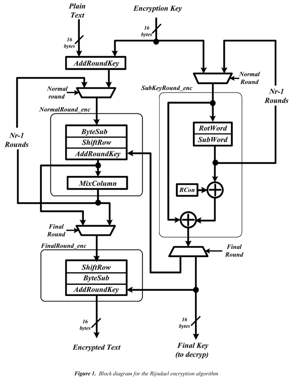
The NormalRound_enc block grouping the four functions of algorithm transformation, is executed Nr-1 times. For its asynchronous description in Balsa, it is not necessary to include the ShiftRow block. This can be implemented through communication of connection lines between the ByteSub and MixColumn blocks. This is possible because the order of the sequential execution of the transformation functions can be changed (Weaver, 2002):
The ByteSub and ShiftRow transformations commutes, which means, a ByteSub transformation followed by a ShiftRow transformation is equal to a ShiftRow transformations followed by a ByteSub transformation.
The column transformation function MixColumn is linear regarding the entrance of the column; which means:
MixColumn (state matrix XOR round key) = MixColumn (state matrix) XOR MixColumn (round key)
These two properties allow inverting the sequence order of the ByteSub and ShiftRow transformations. The order of the AddRoundKey and MixColumn transformations can also be reversed whenever the columns of the encryption key are modified through the MixColumn transformation. The RondaFinal_enc block groups the ShiftRow, ByteSub and AddRoundKey functions.
2.1.1. Byte substitution function: ByteSub
Optimizing the hardware implementation of the ByteSub function is one of the biggest challenges for the Rijndael algorithm designers. According to the FIPS-197 standard (FIPS, 2001), the ByteSub transformation is a substitution non-lineal of bytes that operates independently on each byte of the state matrix, using the substitution table known as Sbox.
Due to the transformation at a byte level, a parallel architecture requires 20 Sbox tables operating simultaneously (16 for the data's block, and 4 for the key). It has been found that an Sbox occupies a big area and consumes a lot of power of the AES circuit; hence most of the design efforts have been focused on getting architectures solving the problem from different viewpoints. In the literature, there are two main approaches to design Sbox circuits (Morioka, 2003): the first one allows getting fast implementations; it consists in creating a single combinatorial circuit, whose input/output relationship is equivalent to the Sbox. Some models of implemented Sbox using this method are PPRM (Positive Polarity Reed Muller) (Morioka, 2003), BDD (Binary Decision Diagram) (Bryant, 1986), or twisted-BDD (Morioka, 2004). The second method allows to use mathematical theorems on Galois Field (FG) to achieve reductions in the circuit area; it consists in making a circuit that implements the function multiplicative inverse, and other circuit for the affine transformation and then, connecting in serial both circuits (Guajardo, 2004). An example of this methodology is the composedfield inversion (Rudra et al., 2001), (Sato et al., 2001) which is based on the idea of transforming the original field GF(28) in a field formed by smaller fields GF((24)2).
However, a study of power consumption of the AES components implemented with libraries of Standard Cells of 0.13µm to composedfields (Morioka, 2003), shows that the ByteSub operation (for 16 Sbox), in a parallel architecture that performs a round per clock cycle, consumes approximately the 75% of the total power circuit. In this research it was found that the main reason for the high power consumption of the Sbox of composite field, is determined by the creation and dispersion of dynamic risks due to the use of complicated signal paths, and the dispersion of signal transitions related to the type of logic gate, particularly for the use of XOR gates.
In order to avoid problems caused by dynamic risks appears the idea to implement the PPRM multi-stage (Morioka, 2003) architecture in asynchronous way. When the asynchronous design is used the dynamic risks problems are eliminated. That is due to the asynchronous style based on models insensitive to delays, in which the correct operation of a circuit does not depend on delays associated to its components. Based on the Sbox PPRM architecture, the Sbox architecture was implemented to encryption. Figure 2 shows a block diagram that indicates the asynchronous communications through the handshake protocols between the modules that compose the Sbox PPRM. The handshake protocol can be of two or four phases, while the codification can be 'singlerail', 'dual-rail' type, or 1-of-4 with technology of QDI circuit.
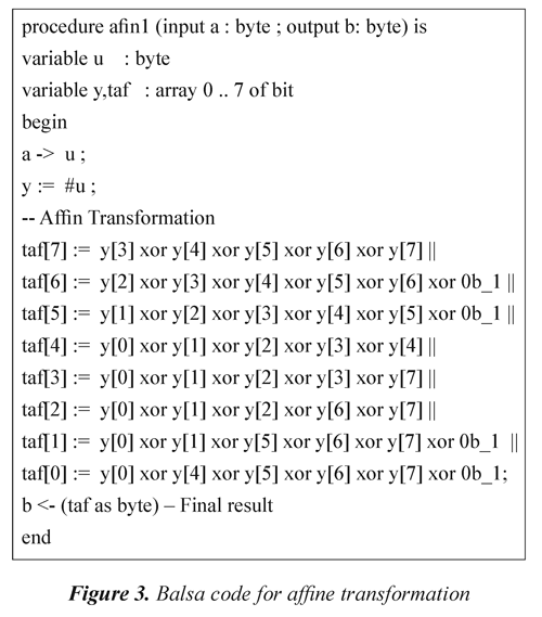
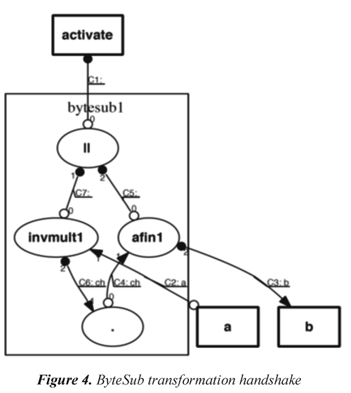
Figure 3 shows, as an example, the code that specifies the module of an affine transformation in Balsa language. Figure 4 shows a handshake diagram generated by the Balsa system after the code synthesis for ByteSub. In general, the handshake diagrams generated by Balsa after compilation of the code description of each circuit, are quite complex since they reflect different signal transitions in each of them. For this reason, in this paper the original handshake diagrams will be omitted hereafter.
2.1.2. ShiftRow function
According to the FIPS-197 (FIPS, 2001) in the ShiftRow transformation, the bytes of the last three rows from the state matrix move cyclically on different number of positions, or offsets. The first row does not move; the 2, 3 and 4 rows move 1, 2 and 3 positions to the left respectively, forming the new state matrix. The ShiftRow function may be implemented in hardware in a simple way through interconnection lines without needing additional components of hardware.
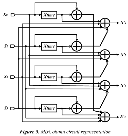
2.1.3. MixColumn function
This function operates column by column on the state matrix and handles each column as a polynomial of four terms. The columns are considered as polynomials GF(28), and module multiplied x4 + 1 with a set polynomial given by:
c(x)= {03}x3 + {01}x2 + {01}x + {02} (1)
This may be written as a multiplication of matrices, in the following way:
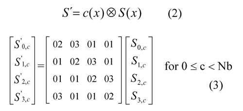
The bytes of each column can be replaced by the result of multiplications according to the following expressions:
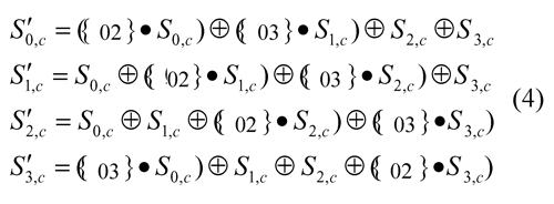
Eq (4) shows polynomial multiplications by powers of x in GF(28). These operations are multiplications of modulus by an irreducible binary polynomial Grade 8 [3]. For Rijndael, this polynomial is called m (x) and is given by
m(x)= x8 + x4 + x3 + x + (5)
To facilitate the implementation of the MixColumn transformation in hardware, the algorithm authors defined the function called xtime, which simplifies the operation of a polynomial by power of x.
Eq. (4) together with the correct use of the xtime function, allows to obtain the circuit that performs the MixColumn function, and whose representation is shown in Figure 5.
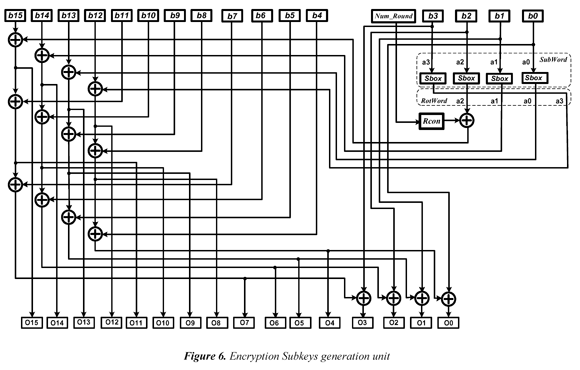
2.1.4. Encryption key generation unit
The key unit circuits included in this section are based on the description made by the Rijndael algorithm authors (Daemen, 1999). The AES algorithm takes the encryption key, K, and performs a spread routine to generate an extended key. The spread routine generates (Nr+1) words: the algorithm requires an initial set of Nb words, and each of Nr rounds requires Nb words of key data. The resulting extended key consists of a lineal arrangement of four bytes, denoted by [wi]: i within the range 0 ≤ i ≤ Nb* (Nr + 1)
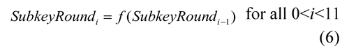
For AES-128 standard (FIPS, 2001), the initial key of 128 bits needs to be extended to 4*(10+1), it means 44 words of 32 bits. That is equivalent to 11 keys of 128 bits. The initial key is the encryption key, and it is used in the initial round of the algorithm. The following keys are derived from the previous key, according to the function f as:
The initial key is represented as a linear arrangement W , in which the round sub-keys are gotten of the initial key, K 0:

Figure 6 represents the circuit for the key expansion unit for an AES-128 encryption algorithm. Figure 6 also shows what the less significant column of the sub-key matrix (column 4) is transformed in different ways to the other columns of the key. Through Sbox, it is applied to the column the SubWord transformation (equivalent to a substitution of byte for each element of column). The resulting column is modified though a circular rotation of position, so that the most significant byte of the column becomes the less significant. The next function is Rcon (addition of round constant), and it consists in performing a XOR operation between a vector column { k r,0,0,0}, and the resulting column. The kr value byte (round constant) depends on the round number that is carried out. The transformations of this column are similar to the encryption and decryption processes.
3. Results and discussion
To estimate the occupied area by each handshake circuit, the Balsa breeze-cost utility has been used in all designs. The units returned by the breezecost are micrometers (µm) cell line on a 1µm 2LM standard CMOS process (Edwards et al., 2006). Balsa supports 350?m and 180?m AMS and SGS-ST technologies, which generate netlist formats to produce implementations on silicon. Balsa also supports the appropriate technology to produce formats used in Xilinx FPGAs.
Table 1 shows the results of implementations simulated using the system Balsa. It relates the cost of relative area and delay time of the functional simulation for each procedure involved in the design of the Rijndael algorithm asynchronous hardware. Balsa generates the area cost as a guide for the designer to know what proportion of a change in the description of a circuit affects its size. For implementation in FPGA, Balsa creates a file compatible with a Verilog specification for each asynchronous circuit. The Verilog file is then synthesized using the software Xilinx Integrated Software Environment (ISE) version 9.2i.
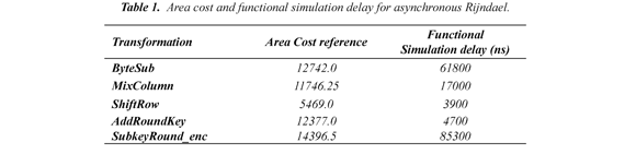
Table 2 shows results of estimated values utilization of the FPGA after Rijndael functions synthesis.
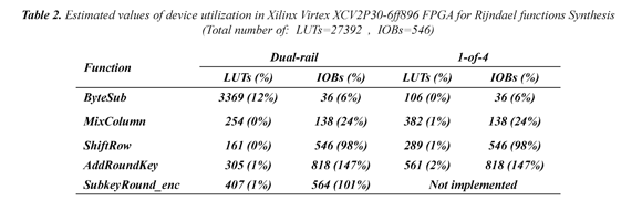
It can see that the most used resource of the FPGA corresponds to IOBs. In some cases (functions AddRounKey and SubKeyRound_enc) the synthesis tool generates IOBs (Input Ouput Blocks) over-mapped when exceeding the required amount of them for assignment of both inputs and outputs necessary in the implementation of the algorithm functions. Table 2 also shows that the percentage of use of Look Up Tables (LUTs), in both types of data encoding, is lower than the percentage of use of IOBs; in addition, the designs require more LUTs when functions are synthesized by using the encoding 1-of-4.
Table 3 shows the results of the real asynchronous implementation in a Xilinx Virtex-II Pro XCV2P30-6ff896 FPGA with 0.13µm CMOS technology and using encryption either dual-rail or 1-of-4 balanced codification.
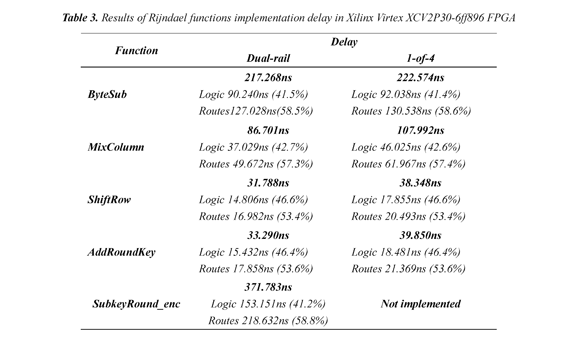
The implementation results in Table 3 indicate that in both styles of coding, the delays associated with asynchronous components interconnection paths are larger than the delays induced by the logic circuit.
The data shows that the interconnection routes have the highest percentage of the total delay of each stage (between 53.4 and 58.6%), which in this case indicates that the FPGA is not used with sufficient interconnection resources suitable for asynchronous design requirements. The results also show that automatic routing algorithms of the system Xilinx ISE are not optimized for interconnections between asynchronous components. Both cases point out as that the current state of Xilinx FPGAs and its design environment has not been oriented to the efficient implementation of asynchronous circuits; however, this is the only available tool for automatic FPGAs synthesis that shows a significant integration level with the Balsa system.
Table 3 also contains the delay times of the encryption key scheduler (SubkeyRound_enc). It was found that the Balsa system does not generate synthesized Verilog files for circuit specification codes 1-of-4 containing table definitions; in this case only the circuits with dual-rail encoding were implemented because of the SubWord function, which is part of both circuits of key generation, including tables to implement the Sbox for byte substitution.
Table 3 shows delay times corresponding to the specifications of the circuit comprising the Rijndael algorithm for encryption as described in section 2.1. Although the FPGA used has enough logic resources and input/output blocks to implement the algorithm, the interconnection resources have proved inadequate for the connectivity of the functions that comprise it.
4. Conclusions
It has been achieved the asynchronous implementation of the functions that make up the Rijndael algorithm. The implemented asynchronous circuits demonstrate a good integration between the asynchronous tool Balsa and the Xilinx ISE 9.2i development platform. However, it is clear that FPGAs used to implement the circuits, have restrictions to map asynchronous circuits. Results obtained with the synthesis tool Xilinx ISE 9.2i, show that the circuits implemented in FPGA have a bigger interconnection routes delay (over 58%) than the logical elements composing each function.
The implementation of the algorithm could be made in the near future using FPGAs with higher-capacity or allowing asynchronous interconnectivity between asynchronous logic blocks, the above must be accompanied by the use of tools with greatest ability to synthesize and to adapt asynchronous digital circuits.
5. References
Bardsley, A. (2000). Implementing Balsa handshake Circui ts . Ph.D. Doctoral Thesis, Faculty of Science and Engineering, University of Manchester, England. [ Links ]
Bouesse, F., Renaudin, M., Wilton, A., & Germain, F. (2005/09/12-16). A clock-less low-voltage AES crypto-processor. In IEEE. Solid-State Circuits Conference, 2005. ESSCIRC 2005. Proceedings of the 31st European (pp. 403-406). New York: IEEE. [ Links ]
Bryant, R.E. (1986). Graph-Based Algorithms for Boolean Function Manipulation. IEEE Transactions on Computers , C-35 (8), 677-691. [ Links ]
Daemen, J., & Rijmen V. (1999). AES Proposal: Rijndael. Proton Worl Int. I, Zweefvliegtuigstraat , Document V. 2. Brussel, Belgium: Katholieke Universiteit Leuven, ESAT-COSIC, Heverlee, Belgium. [ Links ]
Edwards, D., Bardsley, L., Janin, L., & Toms, W. (2006). Balsa: a Tutorial Guide. Version 3.5.The Advanced Processor Technologies Group, APT Group . Manchester: Manchester University. [ Links ]
FIPS, Federal Information Processing Standards, (2001/11/26). Specification for the ADVANCED ENCRYPTION NIST STANDARD (AES) . Publication 197 http://csrc.nist.gov/publications/ [ Links ]
Guajardo, M. (2004). Arithmetic Architectures for Finite Fields GF(pm) with Cryptographic Applications . Dissertation, Doktor-Ingenieurs der Fakultätfür Elektrotechnik und Informations technikan der Ruhr-Universität Bochum von aus Caracas, Venezuela. Bochum. [ Links ]
Morioka, S., & Satoh, A. (2004). A 10-Gbps Full-AES Crypto Design With a Twisted BDD S-Box Architecture. IEEE Transactions on Very Large Scale Integration (VLSI) Systems , 12 (7), 686 - 691. [ Links ]
Morioka, S., & Satoh, A. (2003). An Optimized S-Box Circuit Architecture for Low Power AES Design. Cryptographic Hardware and Embedded Systems (CHES 2002) , 2523, 172-186. Recovered 2015/01/20 http://download.springer.com/static/pdf/334/chp%253A10.1007%252F3-540-36400-5_14.pdf?auth66=1422715307_136548717f28ff8cd1ff51a5b078d8a1&ext=.pdf [ Links ]
Nieto, R. (2009). Diseño e implementación de un cripto-procesador asíncrono de bajo consumo basado en el algoritmo de Rijndael . Doctoral Thesis, Facultad de Ingenierías, Universidad del Valle, Cali, Colombia. [ Links ]
NIST, National Institute of Standards and Technology. (2000). National Institute of Standards and Technology . Recovered 2013/12/15 http://csrc.nist.gov/ [ Links ]
Rudra, A., Dubey, P.K., Jutla, C.S., Kumar, V., Rao, J.R., & Rohatgi, P. (2001). Efficient Rijndael encryption implementation with composite field arithmetic. In CHES. Proc. Cryptographic Hardware and Embedded Systems (CHES 2001) . Lecture Notes in Computer Science (vol. 2162) (pp. 175-188). Paris, France: CHES. [ Links ]
Satoh, A., Morioka, S., Takano, K., & Munetoh, S. (2001). A Compact Rijndael Hardware Architecture with S-Box Optimization. Advances in Cryptology - ASIACRYPT 2001 , Lecture Notes in Computer Science (vol. 2248). (pp. 239-254). Recovered 2015/01/20 http://download.springer.com/static/pdf/373/chp%253A10.1007%252F3-540-45682-1_15.pdf?auth66=1422720654_e9fbf543ebe9797204c9177961a5229d&ext=.pdf [ Links ]
Shang, D., Burns, F., Bystrov, A., Koelmans, A., Sokolov, D., & Yakovlev, A. (2004). A Low and Balanced Power Implementation of the AES Security Mechanism Using Self-Timed Circuits. Integrated Circuit and System Design. Power and Timing Modeling, Optimization and Simulation, Lecture Notes in Computer Science (vol. 3254) (pp. 471-480) Recovered 2015/01/20 http://link.springer.com/chapter/10.1007/978-3-540-30205-6_49 [ Links ]
Shang, D., Burns, F., Bystrov, A., Koelmans, A., Sokolov, D., & Yakovlev, A. (2006). Highsecurity asynchronous circuit implementation of AES. IEE Proceedings Computer Digital Technology , 153 (2), 71-77. [ Links ]
Sui. Ch., Wu, J., Shi, Y., Kim, Y., & Choi, M. (2011/08/7-10). Random Dynamic Voltage Scaling Design to Enhance Security of NCL S-Box. In IEEE. IEEE 54th International Midwest Symposium on Circuits and Systems (MWSCAS) (pp. 1-5). Seul, Corea: IEEE. [ Links ]
Weaver, N., & Wawrzynek, J. (2002). High Performance, Compact AES Implementations in Xilinx FPGAs . New York: U. C. Berkeley BRASS group. [ Links ]
Wu, J., Shi, Y., & Choi, M. (2011/05/10-12). FPGAbased Measurement and Evaluation of Power Analysis Attack Resistant Asynchronous S-Box. In IEEE. Instrumentation and Measurement Technology Conference (I2MTC) (pp. 1-6). Binjian, China: IEEE. [ Links ]

Revista Ingeniería y Competitividad por Universidad del Valle se encuentra bajo una licencia Creative Commons Reconocimiento - Debe reconocer adecuadamente la autoría, proporcionar un enlace a la licencia e indicar si se han realizado cambios. Puede hacerlo de cualquier manera razonable, pero no de una manera que sugiera que tiene el apoyo del licenciador o lo recibe por el uso que hace.
