


Serviços Personalizados
Journal
Artigo
 Inglês (pdf)
 Artigo em XML
 Referências do artigo
 Enviar este artigo por email
Indicadores
-
 Citado por SciELO
 -
 Acessos
Links relacionados
-
 Citado por Google
 -
 Similares em
SciELO
Similares em
SciELO -
 Similares em Google
Compartilhar

 Permalink
TecnoLógicas
versão impressa ISSN 0123-7799versão On-line ISSN 2256-5337
TecnoL. vol.20 no.39 Medellín maio/ago. 2017
Artículo de investigación/Research article
<Microfabrication of position reference patterns onto glass microscope slides for high-accurate analysis of dynamic cellular events
Microfabricación de patrones de referencia en posición en portaobjetos de microscopio para el análisis de alta precisión de eventos celulares dinámicos
July A. Galeano1, Patrick Sandoz2, Artur Zarzycki3, Laurent Robert4, and Juan M. Jaramillo5
1 PhD Engineering, Ingeniería de Sistemas, Grupo de Investigación en Materiales Avanzados y Energía MatyEr, Línea Biomateriales y Electromedicina, Facultad de Ingenierías, Instituto Tecnológico Metropolitano, Medellín-Colombia, julygaleano@itm.edu.co
2 PhD Chargé de Recherche C.N.R.S., Department of Applied Mechanics, FEMTO-ST Institute, University Bourgogne Franche-Comté, CNRS/UFC/ENSMM/UTBM, Besancon-Francia, psandoz@univ-fcomte.fr
3 PhD Engineering, Ingeniería Electromecánica, Grupo de Investigación en Automática, Electrónica y Ciencias Computacionales, Línea Sistemas de Control y Robótica, Facultad de Ingenierías, Instituto Tecnológico Metropolitano, Medellín-Colombia, arturzarzycki@itm.edu.co
4 PhD Ingénieur de Recherche, FEMTO-ST Institute, University Bourgogne Franche-Comté, CNRS/UFC/ENSMM/UTBM, Besancon-Francia, lrobert@femto-st.fr
5 PhD Engineering, Grupo de Investigación Electromagnetismo Aplicado, Línea Microingeniería, Universidad EAFIT, Medellín-Colombia, jjaram44@eafit.edu.co
Fecha de recepción: 28 de marzo de 2017/ Fecha de aceptación: 03 de mayo de 2017
Como citar / How to cite
J. A. Galeano, P. Sandoz, A. Zarzycki, L. Robert and J. M. Jaramillo, “Microfabrication of position reference patterns onto glass microscope slides for high-accurate analysis of dynamic cellular events”, TecnoLógicas, vol. 20, no. 39, 2017.
Abstract
Glass microscopes slides are widely used as in situ base-substrates carrying diverse micro-fabricated systems or elements. For such purposes, the micro-fabrication process consists in transferring a pre-defined design onto the substrate made of a glass microscope slide. This is known as patterning, which is a technique that can also be used in transferring specific designs that allows region of interest (ROI) recovery under the microscope. In those cases, two main challenges appear: 1) Disturbances in light transmission should remain minimum to keep the high quality of observation of the object of interest under the microscope. 2) The pattern-size should then be small enough but, however, larger than the diffraction limit to be observable satisfactorily for positioning purposes. In this article, we present the procedures involved in the microfabrication of Pseudo-Periodic Patterns (PPP) encrypting the absolute position of an extended area. Those patterns are embedded in Pétri dishes in order to allow the high-accurate retrieval of absolute position and orientation. The presented microfabrication is based in a technique known as lift-off, which after parameter adjustment, allows the obtaining of PPP fulfilling the two previously mentioned requirements. The results report on PPP realized on glass microscope slides and composed by 2µm side dots made of aluminum with a thickness of 30nm.
Keywords: Microtechnology, lift-off process, pseudo-periodic patterns, glass microscope slides, micropatterning.
Resumen
Los portaobjetos de microscopio se utilizan ampliamente como sustratos base in situ para la realización de diversos sistemas o elementos microfabricados. Para estos fines, el proceso de microfabricación consiste en transferir un diseño predefinido sobre el sustrato correspondiente a una lámina de vidrio utilizada como portaobjetos de microscopio. Este proceso se conoce como “patterning”, que es una técnica que también se puede utilizar en la transferencia de diseños específicos que permite la recuperación de una región de interés (ROI) bajo el microscopio. En estos casos, aparecen dos desafíos principales: 1) Las perturbaciones en la transmisión de la luz deben permanecer mínimas para mantener la alta calidad de observación del objeto de interés bajo el microscopio. 2) El tamaño del patrón debe ser entonces suficientemente pequeño, pero, sin embargo, mayor que el límite de difracción para ser observable satisfactoriamente para propósitos de posicionamiento. En este artículo presentamos los procedimientos involucrados en la microfabricación de Patrones Pseudo-Periódicos (PPP) los cuales encriptan la posición absoluta de un área extendida. Esos patrones están embebidos en placas de Pétri para permitir la recuperación absoluta y de alta precisión de una ROI, al igual que su orientación. La microfabricación presentada se basa en una técnica conocida como “lift-off” que, tras el ajuste de parámetros, permite la obtención de PPP cumpliendo los dos requisitos anteriormente mencionados. Los resultados corresponden a la realización de PPP en portaobjetos de vidrio y compuesto por puntos laterales de 2µm hechos de aluminio con un grosor de 30nm.
Palabras clave: Micro-tecnología, proceso lift-off, patrones pseudo-periódicos, láminas cubre-objetos de vidrio, micropatterning.
1. Introduction
Glass microscope-slides are widely used by biologists in order to observe, analyze, and quan-tify cellular events and biological samples. Given their uses and its physical properties, microscope slides are used nowadays as base-substrates for the development of microfabrication-based devices such as microfluidics and Lab-on-a-Chip [1]–[4]. The fabrication of those devices requires a previous step of micropatterning. This consists in transferring a pre-defined design onto the substrate by means of techniques such as mask UV-lithography, mask-less lithography systems such as laser-direct-writing-lithography, and inkjet printing [5], [6]. The design corresponds, in most of the cases, to micrometric features. The use of any of the above-mentioned techniques depends on the capacities of the micro-technological facility, being mask-less lithography a more flexible technology allowing the fabrication of shapes with a minimum feature size as small as a few nanometers [7], [8].
Micro-patterning can also be used in applications that implies a simple pattern-transfer direct-ly onto the microscope slide, without the need of embedded electronics. This is the case of applications where region of interest (ROI) recovery is needed either for absolute alignment or for cell-migration quantification and follow-up. In these cases, the micrometric features allow the absolute localization of the observed areas with diverse ranges of resolution and accuracy with respect to the whole substrate. Such image registration is indispensable to document the dynamic changes occurring in live cell cultures over time.
For ROI recovery, different approaches have been proposed, most of them corresponding to alpha-numeric patterns that, once embedded in Pétri-dishes or microscopes-slides, offer a visual way for ROI positioning. Although those types of patterning are nowadays commercial-ized and used by many biologists, the allowed performances are coarse and constitute a major limiting factor for high-accurate analysis of cellular events. This problem has been addressed by diverse authors who proposed several approaches that, in most cases, require the patterning of small-sized features [9]–[13]. As an example, we can reference the pat-tern presented by Dominic et al. [9]. This pattern consists in a variable width line reference grid in order to uniquely characterize every intersection, and at the same time every position, within a working surface.
In our case, we proposed to transfer specific pseudo-periodic patterns (PPP) onto the ground side of Pétri-dishes. The PPP consists of a regular distribution of 2µm sized dots where some of them are absent. The pseudo-periodic distribution allows further Fourier processing for high-accurate but relative positioning, while the absence/presence of dots correspond to an encrypted binary code that allows absolute but coarse positioning. Different from the mentioned approaches, our method also allows orientation measurement. The principle of the method proposed to retrieve a zone of interest under microscope is presented in [14].
The main challenges in microscopes slide patterning are: 1) to obtain a configuration where it is possible to obtain the minimum of losses in light intensity while observing under microscope [15], 2) obtain patterns size close to the diffraction limit of the light in accordance with the lens used in practice, in this case 2µm with classical UV-lithography process, in order to guarantee high-resolution positioning measurement. The small thickness of the substrate (~120µm) makes also challenging to comply with the fragility of the samples.
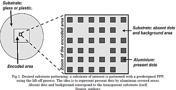
In order to confront the previous mentioned challenges, the patterning of cell-culture dishes presented in this work was done using micro-technology procedures, specifically through an adapted lift-off process. The procedure consisted in patterning a glass microscope cover-slip, which was then inserted in a plastic Pétri dish. The desired patterning is as presented in Fig. 1. The idea is to form a picture of the designed PPP, [14], [15], over the surface of the glass microscope cover-slips (the substrates). The PPP will be formed with aluminum where the present dots correspond to the aluminum covered areas, while the absent dots and back-ground is the transparent substrate itself.
This article presents the procedure of microfabrication of those PPP, indicating the obtained results as well as the issues encountered. During the following subsections, we present the technological procedure to follow in lift-off for substrate patterning.
2. Materials and methods
2.1 Technological realization of PPPs
Lift-off is one of the common processes of patterning a substrate using a metal layer. It does not require special aggressive etchants, which in our case would destroy the substrate. It is quite simple and gives good results. In general, the lift-off method comprehends the following steps: photolithography, metallization, resist stripping and metal lift-off. Below, each step is described in more details. Firstly, however, we present the mask, which is necessary to perform photolithography [16], [17].
2.2 A photolithography mask
A photolithography mask is a piece of glass containing on one side geometric features that are either transparent or non-transparent to UV light. Those features form the pattern that is desired to be reproduced by photolithography, in our case a PPP. For the patterning of the substrates used in this work, we designed a mask in order to be used in negative photolithog-raphy procedures (described in the following items). The mask was designed and elaborated in a chromium-covered silica glass slide.
2.3 Photolithography
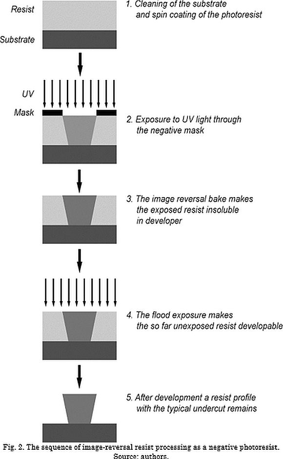
Photolithography is the basic process in microfabrication. The process corresponds to a pattern transfer from a mask onto a substrate covered by UV- sensitive photoresist. For this, three types of photoresist can be used: positive, negative and image reversal. In all the cases, the photoresistcovered substrate is exposed to UV-light through a mask. The diverse process is based on the different reaction of the exposed areas versus non-exposed areas. The main difference in those types of photoresist are explained as follow: in positive photoresist, the exposed areas in the photoresist are removed during the development step while the unexposed areas remain; in negative photoresist the reverse result is obtained: the exposed areas in the photoresist remain while the unexposed areas are removed during the development step. Results obtained with reversal photoresist can be like those from positive or like from negative photoresist, depending on the applied procedure. In our case, for PPP patterning, we used the last mentioned photoresist.
Due to very small elementary dimensions of the desired pattern (grid of squares of 2 µm edge's length) a photoresist characterized by extended resolution capabilities was used, in our case TI09XR [16], which is an image reversal type photoresist. This image reversal type photoresist was used in a negative way over the glass-slides substrates. In this way, a negative mask was designed and used. The procedure of photolithography onto the mentioned substrate is depicted in Fig. 2 and involve the following steps:
1. Process starts from coating the substrate by photoresist layer, TI09XR, of about 700 nm thickness. This is done by a spin coating method with parameters as follow: speed - 4000 r/min, acceleration: 4000 r/min/s, time: 30 sec. After that, photoresist is subjected to soft bake; substrates are put on a hot plate for 50 secs at a temperature of 100°C.
2. In the second step, photoresist is exposed to UV light with dose of 45 mJ/cm². Expo-sure is done through the negative mask.
3. After exposure, the photoresist is subjected to reversal bake. During the reversal bake, the exposed resist areas are converted and become insoluble in the developer, while the resist so far unexposed remains without any changes and can be exposed later. Reversal bake is done on a hot plate for 1 min at a temperature of 130 °C.
4. The fourth step consists in the flood exposure of photoresist with dose of 190 mJ/cm². For this exposure we do not use any mask. The flood exposure makes previously un-exposed areas soluble in developer.
5. The last, fifth step, is development. As in previous process, we immerse the substrate in standard developer MF-26A for 35 sec. During development, areas exposed first remain whereas unexposed are stripped.
One must notice a negative profile of the photoresist's walls. A negative profile means that the pattern width is smaller at its bottom than at its top, which is typical for negative photo-resists.
2.4 Metallization
There are two ways to perform metallization on a substrate: evaporation and sputtering. During the evaporation process, the substrate is placed in a high vacuum chamber at room temperature. The chamber has a crucible, placed under the substrate, that contains the ma-terial to be depositedaluminum, in our case. The crucible is then heated causing the material to evaporate and condense on all the exposed cooler surfaces of the substrate and vacuum chamber as well.
In the case of sputtering, the substrate and a target (the material to be deposited) are placed in a vacuum chamber. Plasma is generated in a side gas source in the chamber, and the ion bombardment is directed towards the target. This causes material to be sputtered off the target and condense on the substrate.
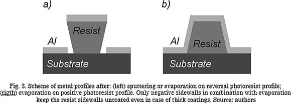
For lift-off purposes, metal deposition by evaporation gives much better results. Evaporated aluminum spreads out from the source radially. It falls perpendicularly onto the substrate's surface due to the significant distance from the target source. This causes the photoresist's sidewalls with negative profile to remain clear (Fig. 3). In the case of a positive profile, the sidewalls would be slightly covered. On the other hand, during sputtering, metal spreads out from the target in a very chaotic way. Moreover, the target is bigger in diameter than the substrate and much closer to the substrates surface. As a result, particles of aluminum land everywhere and create a continuous layer. Metal is deposited even on the photoresist's sidewalls with negative profile. Nevertheless, the thickness of the metal layer on them is negligible. We used evaporation to fabricate PPPs. The thickness of the aluminum in the PPPs ranged from 30 nm to 100 nm.
In future works it will be important to consider the use of other metals for the PPP. The point is achieving sufficient opaqueness and light budget ensuring the correct acquisition of cell images under the microscope. Two parameters greatly determine the opaqueness level: the thickness of the metal on the microscope slide and the extinction coefficient of the material. As presented in [8], the light budget can be estimated from the dots transparency and the configuration of the PPP (the number of dots in the field of view). We calculated a light budget of 85%, for the aluminum and PPP configuration used in this work. This value was enough for the application.
2.5 Lift-off
Finally, the lift-off step is performed. Substrate is immersed in a liquid made of a powerful photoresist solvent that is chemically inert on glass and metal. Once the dissolved photoresist is stripped out from substrate, the aluminum layer over it is lifted-off, while the metal deposited directly on the substrate remains. Remaining areas of aluminum form the final PPP on the substrate.
3.Results
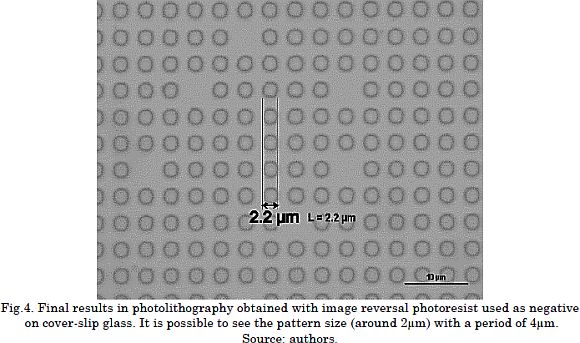
Final results are presented in Fig. 4 for the photoresist patterning on coverslip glasses using image reversal photoresist as a negative one.
3.1 Technological problems
There are some problems that can be encountered during photolithography. In our case, the principal problems that affected the process were related to substrate resist mask adjustment, first exposure dose/reversal bake, and development:
3.1.1 Substrate-resist-mask adjustment
Here we use the word adjustment to make reference to the junction of the substrate (cov-ered by photoresist) with the predesigned mask, for UV exposure. Commercial UV lamps are already equipped with a specific device to perform this adjustment automatically. In our case, manual adjustment is performed due to the particular size and shape of our substrates that make impossible to use the specialized machine available.
3.1.2 First exposure dose
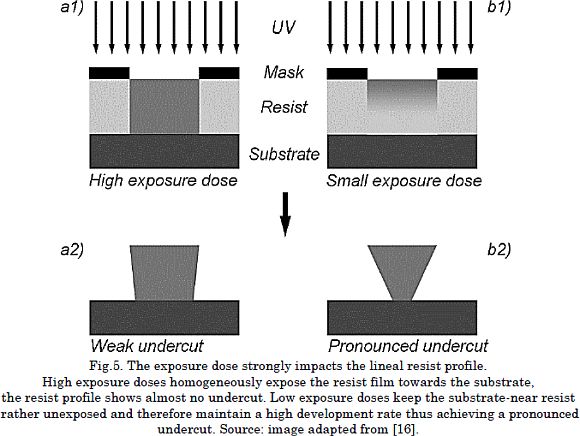
Fig. 5 shows that a high dose during the first exposure (a1) results in a steep resist profile with minor undercut (a2) after reversal bake, flood exposure, and development. Conversely, a low dose during the first exposure (b1) that does not affect the resist layer near the substrate produces a strong undercut and sometimes the peeling of narrow resist structures in the developer (b2). Therefore, the optimum dose of the first exposure depends on the de-sired undercut and the minimum lateral feature sizes [16].
3.1.3 Development
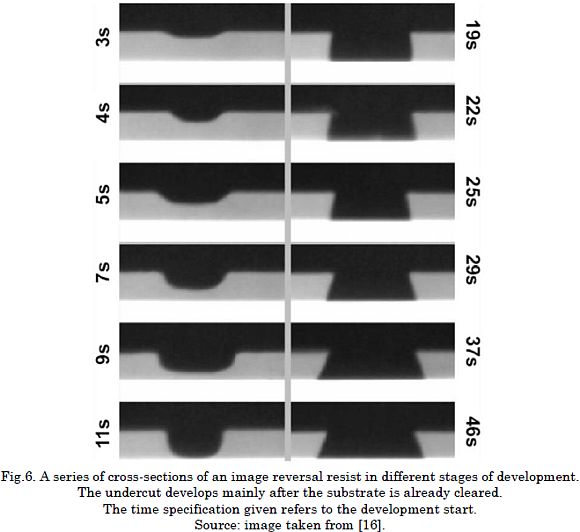
The undercut forms in the last stage of development, according to the development time, are presented in Fig. 6. It is important to use a considerable development time (normally to ob-tain 30% of over-developing) that avoid the presence of photo-resist in the forming undercuts. The presence of photo-resist in the undercuts yields to incorrect patterning of the substrate since the metal will not be deposed directly on the substrate [16].
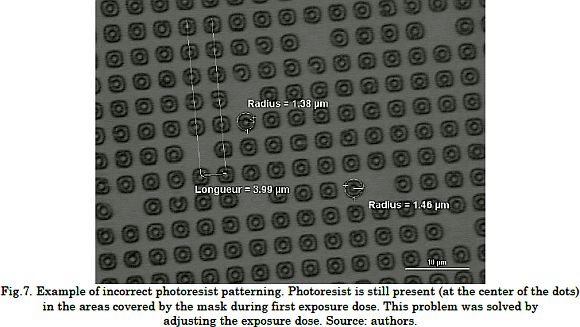
In order to avoid the problems related to exposure dose and development time, several tests were done in clean room in order to find the correct values for acceptable photoresist patterning. As example, Fig. 7 shows a bad photoresist patterning when using a high value in first exposure dose. The problem was solved, after several tests, when using a middle value in first exposure dose (45 mJ/cm²).
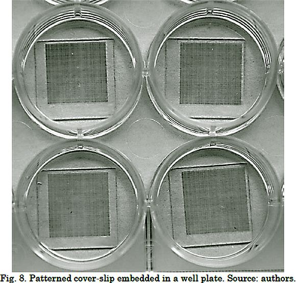
The obtained patterned cover-slips were embedded in Pétri dishes as well as in well plates. A way to do this, was just by gluing them at the external bottom side of the dish (Fig. 8). An-other way is by using PDMS (Poly-Di-Methyl-Siloxane: a biocompatible polymer) in order to cover the glass-cover slips and then gluing it in the internal part of the Pétri dish or plate. For PDMS preparation, we used a standard process that implies the use of the PDMS itself together with a curing agent, as presented in the following [18]:
1. Mix the curing agent with the PDMS, by conserving a weight ratio between them of 1:10.
2. Degas the previous preparation by using a vacuum pump: this in order to remove the bubbles that could be caused during the mixing procedure.
3. Pour the preparation over the PPP substrate.
4. Centrifugate the substrate with the PDMS mixture for 40 secs to obtain a uniform PDMS layer on the substrate.
5. Place the substrate in an oven at 80°C for 8 hours to soft bake the PDMS mixture.
Both, the PDMS layer and the cellculture box thickness form the necessary height distance between the PPP and the biological material to be observed under the microscope. This distance avoids image crosstalk during the image acquisition of either the cell-culture or the PPP. The processing of the PPP image allows to measure in a precise way the position of the cell-culture under observation as reported elsewhere [15].
4. Conclusions
T This paper presents the patterning of glass microscope slides for accurate recovery of the Region of Interest (ROI) form cell cultures. Microscope slide patterning poses two challenges: avoiding light transmittance losses and making the patterns size compatible with the diffrac-tion limit of optical microscopes. In order to overcome these issues, we propose to employ a microfabrication technique known as "lift-off" for patterning glass coverslips. The patterned coverslips are then embedded in Petri dishes to be later used in precise ROI localization.
The lift-off process used in this work comprises the following main steps: photolithography, metallization, resist stripping, and metal lift-off. The photolithography process involves a mask (designed by the authors) composed of a PPP (feature size = 2µm side). This is small enough to minimize light transmission disturbances while sufficiently large to be resolved by midrange numerical aperture lenses. For such small dimensions, a high resolution photoresist must be used. In this work we used TI09XR. The combination of this resist and an appropriate exposure time and dose (45 mJ/cm2) during development ensure a pattern that is small and reliable enough for accurate ROI localization (by suitable image processing techniques). In the case of metallization, the evaporation facilitated the fabrication of 30nm thick aluminum dots. This set of values minimizes the losses of light transmittance during microscope observations. It also aids automatic and highly accurate position retrieval when the patterned slides are placed on Petri dishes or other devices supporting the cell cultures.
Further studies will focus on the development of this kind of patterns for applications in other domains (such as precise control and robotics). They will also address the construction of flexible low-cost lithography machines for the fabrication of such patterns without the need of a mask.
5. Acknowledgments
The authors acknowledge the RENATECH network and its FEMTO-ST technological facility MIMENTO. Also, we acknowledge the financial support given by Instituto Tecnológico Metropolitano (Medellin-Colombia), and by Institute FEMTO-ST (Besancon- France), under the project number P15201.
References
[1] R. Ramji, N. T. Khan, A. Muñoz-Rojas, and K. Miller-Jensen, “Pop-slide patterning: rapid fabrication of microstructured PDMS gasket slides for biological applications,” RSC Adv., vol. 5, no. 81, pp. 66294-66300, 2015. [ Links ]
[2] B. Gumuscu, A. den Berg, and J. C. T. Eijkel, “Custom micropatterning of hydrogels in closed microfluidic platforms fabricated by capillary pinning,” in The 18th International Conference on Miniaturized Systems for Chemistry and Life Sciences, 2014. [ Links ]
[3] J. Lafaurie-Janvore, E. E. Antoine, S. J. Perkins, A. Babataheri, and A. I. Barakat, “A simple microfluidic device to study cell-scale endothelial mechanotransduction,” Biomed. Microdevices, vol. 18, no. 4, p. 63, Aug. 2016. [ Links ]
[4] N. Nagarajan, K. Hung, and P. Zorlutuna, “Protein Micropatterning Techniques for Tissue Engineering and Stem Cell Research,” in Cell and Material Interface: Advances in Tissue Engineering, Biosensor, Implant, and Imaging Technologies, vol. 52, CRC Press, 2015, pp. 109-146. [ Links ]
[5] J. Jaramillo, A. Zarzycki, J. Galeano, and P. Sandoz, “Performance Characterization of an xy-Stage Applied to Micrometric Laser Direct Writing Lithography.,” Sensors (Basel)., vol. 17, no. 2, p. 278, Jan. 2017. [ Links ]
[6] C.-T. Chen, “Inkjet Printing of Microcomponents: Theory, Design, Characteristics and Applications,” in Features of Liquid Crystal Display Materials and Processes, InTech, 2011, pp. 43-60. [ Links ]
[7] K. Boolchandani and B. Sarita, “A Review Paper on Nanotechnology Applications and Concepts,” in IJIRST || National Conference on Innovations in Micro-electronics, Signal Processing and Communication Technologies (V-IMPACT-2016), 2016, pp. 61-62. [ Links ]
[8] A. Nag, A. I. Zia, S. C. Mukhopadhyay, and J. Kosel, “Performance enhancement of electronic sensor through mask-less lithography,” in 2015 9th International Conference on Sensing Technology (ICST), 2015, pp. 374-379. [ Links ]
[9] D. St-Jacques, S. Martel, and T. B. FitzGerald, “Nanoscale Grid based potitioning system for miniature instrumented robots,” in Canadian Conference on Electrical and Computer Engineering, 2003, vol. 3, pp. 1831-1834. [ Links ].
[10]D. B. Boyton, “Position encoder using statistically biased pseudorandom sequence.” 2004. [ Links ]
[11] V. Guelpa, P. Sandoz, M. A. Vergara, C. Clévy, N. Le Fort-Piat, and G. J. Laurent, “2D visual micro-position measurement based on intertwined twin-scale patterns,” Sensors Actuators A Phys., vol. 248, pp. 272-280, Sep. 2016. [ Links ]
[12] M. J. Yao, “Method of printing location markings on surfaces for microscopic research.” 2013. [ Links ]
[13] M. Wrenn and D. Soenksen, “Systems and methods for tracking a slide using a composite barcode label.” 2016. [ Links ]
[14] J.-A. Galeano-Zea, P. Sandoz, E. Gaiffe, J.-L. Pretet, and C. Mougin, “Pseudo-Periodic Encryption of Extended 2-D Surfaces for High Accurate Recovery of any Random Zone by Vision,” Int. J. Optomechatronics, vol. 4, no. 1, pp. 65-82, Jan. 2010. [ Links ]
[15] J. A. Galeano Z., P. Sandoz, E. Gaiffe, S. Launay, L. Robert, M. Jacquot, F. Hirchaud, J.-L. Prétet, and C. Mougin, “Position-referenced microscopy for live cell culture monitoring,” Biomed. Opt. Express, vol. 2, no. 5, p. 1307, May 2011. [ Links ]
[16] M. GmbH, Lithography: Theory and Applications of Photoresists, Developers, Solvents and Etchants. MicroChemicals GmbH, 2007. [ Links ]
[17] M. J. Madou, Manufacturing techniques for microfabrication and nanotechnology, 1st ed., vol. 2. Boca Ratón - Florida: CRC Press, 2011. [ Links ]
[18] Elveflow, “How to do PDMS lithography replication from a su-8 mold: The PDMS lithography replication process: tips and tricks,” The SU-8 mold fabrication process: tips and tricks. [Online]. Available: http://www.elveflow.com/microfluidic-tutorials/soft-lithography-reviews-and-tutorials/introduction-in-soft-lithography/pdms-softlithography-replication/. [ Links ]

