


 English (pdf)
 Article in xml format
 Article references
 Send this article by e-mail
 Cited by SciELO
  Cited by Google
  Similars in
SciELO
Similars in
SciELO  Similars in Google
 Permalink
1. INTRODUCTION
Currently, the energy industry primarily uses non-renewable sources such as petroleum, coal, and natural gas, mainly because transforming fossil fuels into electrical energy is cheaper [1]. However, this is unsustainable because of continuous population growth and technological advances which increase energy consumption, causing increased greenhouse gas emissions and global warming, leaving sustainability at risk. Therefore, global energy demand should be met using zero-emission or renewable energy sources such as solar. For instance, just using photovoltaic modules with a power conversion efficiency of 10 % and using sunlight that reaches 0.1 % of the Earth’s surface would be enough for meeting global needs [2].
CuInSe2 (CISe) or Cu(In, Ga)(S, Se)2 (CIGS) absorber layers are one of the most promising materials for photovoltaic devices that takes advantage of the inexhaustible solar energy source and transforms it into electrical energy without producing pollution during the process. CISe and CIGS absorbers layers exhibit a high absorption coefficient, favorable bandgap, outstanding photoelectronic properties, stability against photodegradation, and PCEs above 23 % [3], [4].
Generally, the highest PCEs in CIGS-based thin-film solar cells have been obtained with the addition of alkali elements (Na, K, Rb, Cs) via vacuum-based technologies (co-evaporation and sputtering), and it seems to follow a tendency of a better solar cell performance going from lighter to heavier alkali elements [5], [6].
Both definitions Na addition effect on CIGS-based solar cells has been studied broadly, it makes the grain morphology smoother with a strong (112) crystallographic plane texture, increasing hole concentration because of the substitution of Incu antisites defects, improving the efficiency, and the p-type absorber layer [7]- [10]. Potassium, on the other hand, enhances the CIGS/CdS interphase by diffusing Cd into the Cu-poor chalcopyrite-based layer which allows obtaining a thinner CdS layer that decreases optical losses [11]. Rubidium addition has demonstrated an increase of carrier concentration, a reduction in crystallinity defects and recombination improving the solar cell’s performance, possibly by grain boundaries passivation [12], [13]. Rubidium causes Cu-deficiency at the CdS/CISe interface and grain boundaries forming a high-bandgap RbInSe2 secondary phase, and cause type inversion through increased Cd2+ penetration into the CISe (forms n-doped CISe at the surface) [14]. In addition, Cesium incorporation on CIGS-based solar cells shown recombination reduction by a valence band downshift and influence the sodium and potassium distribution through the grain boundaries [15]. This alkalis element distribution has been studied by atom probe tomography (APT) techniques. The results shown that the mechanism involves heavier alkalis (Rb or Cs) pushing lighter alkalis (Na or K) out of grain boundaries in the CIGS-absorber layer. This increases open-circuit voltage (Voc) [16] of the device, thus resulting in an increase in the PCEs at the same time.
The above-mentioned CIGS-based solar cells with alkali elements are, however, produced through vacuum methods, and those techniques represent a high cost, which is an obstacle to their manufacture. On the other hand, non-vacuum techniques such as solution-based methods have emerged as an alternative because of their potential for low-cost, highly scalable production, application in flexible substrates, and high PCEs by around 17.3 % [17]. This type of solution-based process with the addition of rubidium alkali has not been sufficiently studied.
To broaden the general understanding of this specific topic, a thermal evaporation post-deposition technique (PDT) is proposed to deposit rubidium on the CISe layer produced via solution-based techniques with a mixture of amine-thiol and to establish its effect on the physical, chemical, and optoelectronic properties of the absorber layer.
2. METHODOLOGICAL ASPECTS
2.1 Synthesis of CISe via molecular precursors
The CuInSe2 films were prepared by dissolving the precursor powders (Cu2Se, In2Se3, Se) in a mixture of butylamine (BA) and ethanedithiol (EDT) at a concentration of 0.17 M Cu, 0.196 M In, and 0.39 M Se. The process was carried out in a glovebox at room temperature and O2(g) levels below 0.1ppm. Additionally, the vessels with the precursor solution were stirred on a hot plate at 35°C for 3 days until a homogeneous and Cu-poor solution precursor ink (Cu/In <1) was obtained.
2.2 Coating process
20 μL of ink per layer was blade-coated on molybdenum-coated (~800 nm) soda-lime glass substrates (2 mm thick) using an Auto Blade Coater (Modified Monoprice Mini V2 3D printer). The samples were then annealed at 300°C for 2 minutes to evaporate the excess solvent and form the crystalline CISe phase. Then, the film was allowed to cool naturally on an aluminum block for 6 minutes, this process was repeated 5 times per sample to obtain the desired thickness.
2.3 Selenization and growth
Before the selenization process, a 10 nm thick layer of NaF was deposited on top of the as-coated films via thermal evaporation. After that, CISe as-coated films were selenized in a tube furnace under a selenium-argon atmosphere. For selenization, the thin films were placed in a rectangular graphite box with the addition of 304 mg of selenium pellets around the film. This box was put inside a tube furnace (preheated) at 500°C for 20 min. Afterward, the graphite box was allowed to cool naturally to room temperature with argon flow inside the tube furnace. The selenized CISe film had a Cu/In ratio of 0.720 ± 0.015, as measured by XRF.
2.4 Thermal Evaporation
Using RbF as the target material in a glovebox bell jar thermal evaporator instrument, RbF layers of 10 nm and 30 nm were deposited on top of the as-selenized CuInSe2 thin film under a pressure of 1.5x10⁻⁵ mbar. After the thermal evaporation process, a second selenization process with the same amount of Se pellets than the previous one was carried out in a tube furnace (preheated) at 350°C for 20 minutes. This process allows rubidium diffusion and the possible formation of desirable phases, such as RbInSe2.
2.5 Devices fabrication
To complete the device, the general arrangement of SLG/Mo/CISe/CdS/ i-ZnO/ ITO/ Ag grids was used. After the CISe-(RbF) absorber layer growth, a 50 nm thick layer of CdS was deposited by chemical bath deposition as a buffer layer. After that, the window layer composed of an i-ZnO layer with an 80 nm layer and indium-doped tin oxide (ITO) of 220 nm were deposited via RF sputtering. For finishing the devices, Ag grids were deposited by thermal evaporation as front contacts.
2.6 Characterization
X-ray fluorescence (XRF) measurements were taken using a XAN 250 He XRF unit which was equipped with a silicon detector, a primary nickel filter, and a collimator operated at a voltage of 50 kV, using Helium gas for displacing air from the data collection pathway.
Using three measurements of 60 seconds for each spot, the atomic composition in each sample was determined. X-ray diffractograms were collected using a Rigaku diffractometer using a Cu Kα (λ = 1.5406 Å) source and 40 kV and 44 mA in parallel beam (PB) mode at an angle of 0.5° as operating conditions. Steady-state Photoluminescence spectrums were measured using a Horiba/JY LabRAM HR800 Raman Microscopy and Photoluminescence Spectroscopy with a 632.8-nm He: Ne laser and an InGaAs detector. Six spots per sample were analyzed. Time-resolved photoluminescence (TRPL) measurements were conducted using a Horiba/Jobin-Yvon Fluorolog (NanoLED light source) with a 637 nm pulse and a voltage of 725 V. Grain size and morphology were analyzed using scanning electron microscopy (SEM) at 5 kV accelerating voltage and around 5mm as a working distance.
3. RESULTS AND DISCUSSION
3.1 Chemical composition and morphology
To obtain high-efficiency CIGS or CISe-based solar cells, a copper-poor composition (Cu/In<1) is required because of the formation of ordered defects or ordered vacancy compounds (OVC/ODC) on the surface. These phases make the CISe surface weakly n-type, and it forms a homojunction with the bulk (p-type). Additionally, this junction decreases the interfacial recombination between the absorber and the buffer layer [18], [19], [20].
As it is depicted in Figure 1, the Cu/In atomic ratio was uniform and below 1, and additionally, the results of the three different samples had a low standard deviation according to the error bars in the graph, which represents the uniform composition of the starting molecular solution method. Moreover, the composition control of Cu-poor materials is crucial for the RbF diffusion [21], [22].
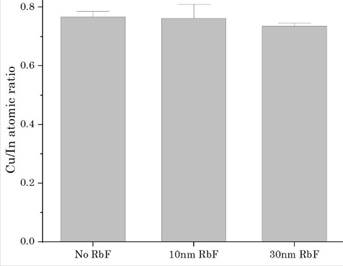
Figure 2 shows top-view scanning electron microscopy images of the CISe absorber layers, and the effect of RbF layers addition after the samples are selenized. It is remarkable the increase in the grain size and morphology changes at the same selenization temperature with the addition of 10 and 30 nm of RbF layers via thermal evaporation.
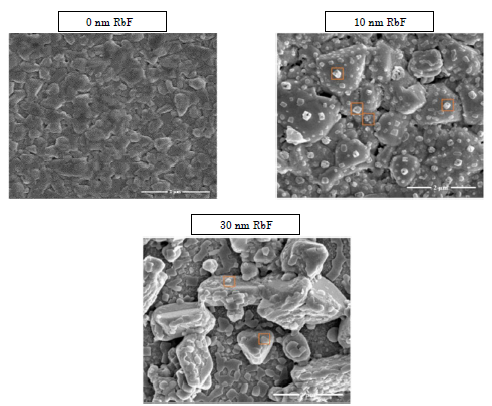
Source: Created by the authors.
Figure 2 Top-view SEM images of CISe-based thin films with different amounts of Rubidium Fluoride addition
These results likely suggest a liquid assisted grain growth process in the films [23]. Additionally, after the PDTs, the surface of the CISe absorber layer is covered with islands (highlighted) which can be mainly composed of Se, Rb, and/or F. Moreover, when rubidium evaporated layers become thicker, the grains start to separate, they show a rough surface and some pinholes are also revealed, this behavior is in agreement with previous studies on post deposition techniques using alkali elements like potassium by post deposition techniques [24]. Regarding crystallinity and phase analysis, X-ray diffraction was utilized.
Figure 3a shows a good match of the theoretical XRD spectrum of the CISe phase and the experimentally obtained CISe without and with the addition of RbF. The main characteristic peak (112) around 27.5° does not vary in position with the RbF addition and shows a preferred crystal orientation which indicates the chalcopyrite phase formation in every single sample. Also, Figure 3b represents the full width at half maximum (FWHM) of the main diffraction plane, which decreases when RbF is added on CISe. It means that with the addition of 10 and 30 nm of RbF there is an improvement in the crystallinity and an increase in the grain size, which is consistent with the previous SEM images of the CISe films.
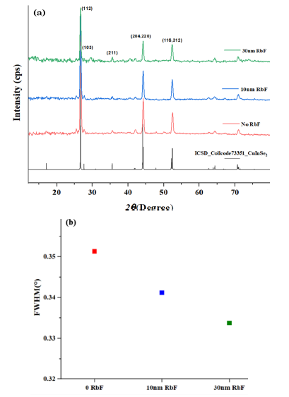
Source: Created by the authors.
Figure 3 a) X-ray diffraction patterns of CISe samples with the addition of RbF. b) FWHM of the main diffraction plane of the CISe tetragonal structure (112)
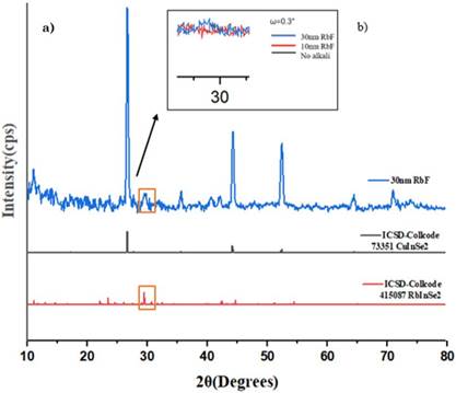
For identifying the general structure and crystallographic phases not just in the CuInSe2 absorber bulk but in its surface where RbF layers were deposited, grazing incidence x-ray diffraction was implemented. An omega angle (ω) in a range from 0.5° to 0.1° was used in most of the samples, where ω= 0.5° represents an analysis depth ~200nm thick. In addition, the chalcopyrite diffraction patterns are observed along the absorber layer bulk.
The possible presence of the RbInSe2 ternary phase was associated with the formation of a peak around 30° which is detected for the samples with 10 and 30nm of RbF as is depicted in Figure 4. Additionally, the RbInSe2 phase is not observed for the sample without RbF addition. The ternary phase is caused by an excess of doping of Rb in the CISe absorber layer at temperatures lower than 800 K as is explained in a research utilizing density functional theory (DFT) by Malitckaya et al. [25].
3.2 Opto-electronic properties
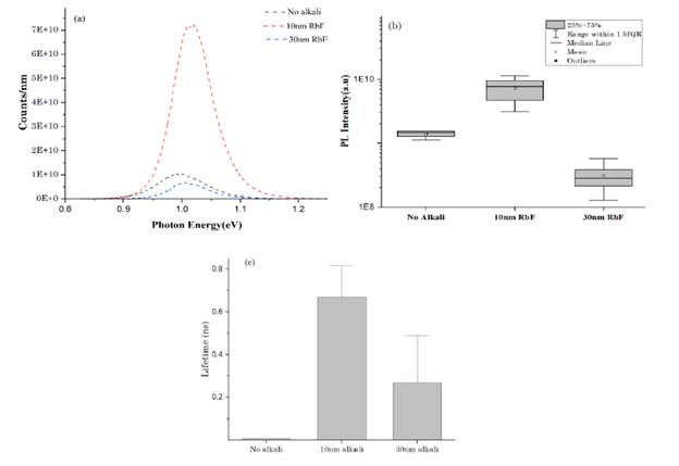
To have a better understanding of the changes in the optoelectronic properties when rubidium fluoride is added, photoluminescence and time resolve measurements were carried out. Figures 5a and 5b show the comparison between the steady state PL intensity and the amount of rubidium fluoride added on top of the CISe thin film. As Figure 5b indicates, with the addition of 10 nm of RbF there is a representative increasing trend in the PL intensity without obtaining outliers values or overlapping the interquartile zone of the boxes between each condition. This higher PL intensity, caused by the passivating effect of rubidium fluoride, could lead to an increase in the quality of the CISe absorber layer, decreasing non-radiative recombination (or defect density), and improving optoelectronic properties. The increased on PL peak intensity with addition of rubidium also has been proved by vacuum methods [26], which supports the utilization of cheaper methods such as solution processing techniques. In addition, with 30 nm of RbF, the PL intensity decreased, this fact can be related to the formation of a barrier in the bulk because of the amount of Rb doping. This result has been reported by E. Avancini et al. [27], adding KF by post-deposition techniques. Additionally, there is a peak shift with the addition of RbF, this suggests the effect of the RbInSe2 ternary phase formation which has a higher bandgap of about 2-2.6eV than the CISe [14].
Source: Created by the authors.
Figure 5 (a), (b) Photoluminescence signals and (c) Time-resolved photoluminescence results for CISe thin films with the addition of RbF
In Figure 5c, time-resolved photoluminescence (TRPL) demonstrated how the addition of RbF by thermal evaporation increases the carrier lifetime of the absorber layer when you add 10 nm of RbF. According to the standard deviation of the data there is not a clear difference when 30 nm of RbF is added on the absorber layer compared to the sample without post treatment. The improvement of carrier lifetime aligns with the photoluminescence results when 10 nm of RbF is added. One of the reasons for data variability in TRP signal is related to the possible several charge carrier dynamics in the absorber layer such as minority charge trapping, material degradation, among others [28].
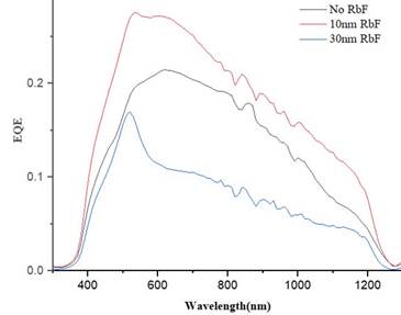
For analyzing electrical properties developed by the addition of RbF in the completed device, external quantum efficiency was utilized. Figure 6 shows how the addition of 10nm of rubidium fluoride increases the ratio of the number of carriers collected by the solar cell to the number of photons entering in a wavelength range from 350 nm to 1250 nm. Also, there is an increase in the blue response which is related to a front surface recombination reduction generated by rubidium fluoride.
Source: created by the authors.
Figure 6 EQE measurements with the addition of RbF; without RbF, 10 nm RbF, and 30 nm RbF
On the other hand, higher doping with RbF (30 nm) reduced the general external quantum efficiency trend in the bulk. This result might be related to previous reports that have shown the same tendency. An excessive amount of RbF results in the formation of a barrier for the injection current, which produces a general decrease in solar cell parameters [27], [29].
4. CONCLUSIONS
In this work, the effect of post deposited rubidium fluoride on CISe-based solar cells was investigated. CISe-based solar cells were deposited by molecular precursors using an amine-thiol mixture and they had a uniform atomic ratio composition around 0.78, which means Cu-poor composition. The crystallinity and grain size of the samples improved with the addition of RbF according to the scanning electron microscopy and x-ray diffraction analysis. Additionally, optoelectronic properties such as photoluminescence intensity and charge carrier lifetime showed an improvement in the collection of minority charge carriers with the addition of 10nm of RbF.
We found that doping chalcopyrite-based solar cells with rubidium can present similar behavior comparing vacuum and solution processing techniques when it comes to the enhancement of charge carrier lifetime, grain size and obtention of a uniform chemical composition. This emphasizes that doing research about the use of solution processing techniques is very relevant since it could facilitate the potential development of chalcopyrite-based solar utilizing low-cost techniques to achieve large-scale production in this technology.

