


Serviços Personalizados
Journal
Artigo
 Inglês (pdf)
 Artigo em XML
 Referências do artigo
 Enviar este artigo por email
Indicadores
-
 Citado por SciELO
 -
 Acessos
Links relacionados
-
 Citado por Google
 -
 Similares em
SciELO
Similares em
SciELO -
 Similares em Google
Compartilhar

 Permalink
Tecnura
versão impressa ISSN 0123-921X
Tecnura vol.18 no.spe Bogotá dez. 2014
https://doi.org/10.14483/udistrital.jour.tecnura.2014.DSE1.a02
DOI: http://doi.org/10.14483/udistrital.jour.tecnura.2014.DSE1.a02
Synthesis and characterization of In(O;OH)S/AgInS2 interface heterojunction
Síntesis y caracterización de interfase de heterojuntura In(O;OH)S/AgInS2
William Vallejo*, Carlos Díaz Uribe**, Carlos Andrés Arredondo***, Mario Alberto Luna****, Johann Hernández*****, Gerardo Gordillo******
* He received his PhD in Chemistry (solar energy materials and solar cells) in 2011 from Universidad Nacional de Colombia. He is an associate professor of Chemistry program at Universidad del Atlántico from 2012. His main research interest areas are synthesis and characterization of PV Materials. williamvallejo@mail.uniatlantico.edu.co
** He received his PhD in Chemistry in 2010 from Universidad Industrial de Santander. He is an assistant professor of Chemistry program at Universidad del Atlántico from 2012; currently, he is director of research group in Photochemistry and Photobiology. carlosdiaz@mail.uniatlantico.edu.co
*** Electrical Engineer, PhD in Physics (solar energy materials and solar cells) from Universidad Nacional de Colombia. Assistant professor of the energy engineering program at Universidad de Medellín from 2012, and researcher of the Grupo de Investigación en Energía - GRINEN of the same university. The main research interest areas are: PV systems and materials for solar cells, and renewable energy systems implementation on rural and urban areas. Medellín, Colombia. caarredondo@udem.edu.co
**** Environmental and Sanitary Engineer, PhD in Environmental Conservation (focused on renewable energy) in 2011 at the Estonian University of Life Sciences from Tartu, Estonia; in 2009 received the master degree in Environmental Sciences and Territory Management at Institute Súperier d´Agriculture from Lille, Francia. Researcher/lecturer at Universidad de Medellín since 2012. The interested work area is focused on the implementation of renewable energy systems on urban and rural areas. Medellín, Colombia. mluna@udem.edu-co
***** Electrical Engineer. MSc and PhD degrees in Electrical Engineering from Universidad Nacional de Colombia in 2007 and 2012, respectively. In 2009 he joined the staff of the Department of Electrical Engineering at Universidad Distrital Francisco José de Caldas, where he works currently as Associate Professor and director member of Laboratory in Alternative Energy Sources (LIFAE). His research interests include power quality, photovoltaic systems, distributed generation, microgrids and energy efficiency. jahernandezm@udistrital.edu.co
****** Bachelor in Physics. MSc in Physics from Universidad Nacional de Colombia in 1974. PhD degree in Electronic-Physics from Stuttgart University, Germany, in 1984. He is currently a professor with the Department of Physics at Universidad Nacional de Colombia. His research fields are thin film photovoltaics devices and photovoltaic generation systems. ggordillog@unal.edu.co
Fecha de recepción: June 10th, 2014 Fecha de aceptación: November 4th, 2014
Citation / Para citar este artículo: Citation / Para citar este artículo: Vallejo, W., Uribe, C. D., Arredondo, C. A., Luna, M. A., Hernández, J., & Gordillo, G. (2014). Synthesis and characterization of In(O;OH)S/AgInS2 interface heterojunction. Revista Tecnura, 18 (Edición especial doctorado), 30-40. doi: 10.14483/udistrital.jour.tecnura.2014.DSE1.a02
Abstract
In this work, we presented some complementary studies for In(O,OH)S thin films deposited on AgInS2 thin films to fabricate a new system absorbent-layer/buffer-layer to be used in tandem and/or in one-junction solar cells. As showed in previous works carried out for us, AgInS2 layers were grown by co-evaporation from metal precursors in a two-step process; and In(O,OH)S thin films were deposited by Chemical Bath deposition. X-ray diffraction measurements indicated that AgInS2 thin film grown with chalcopyrite structure; and In(O,OH)S films grown with polycrystalline structure. The AgInS2 thin films presented p-type conductivity, and from transductance measurements it was found a high absorption coefficient (greater than 104 cm−1) and an energy band gap of 1.95 eV; and In(O,OH)S thin films presented Eg about 3.01 eV; morphological analysis indicated that under this synthesis conditions, In(O,OH)S thin films coated completely the AgInS2 absorber layer. Finally, the Avrami-Erofeev equation was used in this work to study In(O,OH)S thin film growth rate on AgInS2 substrate. Results indicate that the developed system can be used in single-junction and multiple junction solar cells.
Keywords: absorber layer thin film, AgInS2, buffer layer, In(O,OH)S, optic window, solar cells.
Resumen
En este trabajo presentamos estudios complementarios de películas delgadas de In(O;OH)S depositadas sobre películas delgadas de AgInS2 para fabricar un sistema capa absorbente/capa buffer utilizado en celdas solares tipo tándem o celdas de juntura simple. Como se demostró en trabajos anteriores realizados por los autores, las capas de AgInS2 crecieron por coevaporación de los metales precursores en un proceso de dos etapas; y las películas delgadas de In(O:OH)S se depositaron por baño químico. Las medidas de rayos X indican que las películas de AgInS2 crecen con estructura tipo calcopirita y las de In(O:OH)S con estructura policristalina. Las películas de AgInS2 presentan conductividad tipo P, y de las medidas de transductancia se encontró un coeficiente de absorción alto (mayor a 104 cm-1), y un gap de 1.95 eV; las películas de In(O:OH)S presentaron un gap de 3.01 eV; el análisis morfológico indica que bajo estas condiciones de síntesis, las películas de In(O:OH)S recubren completamente la capa absorbente de AgInS2. Finalmente, en este trabajo se aplicó la ecuación de Avrami-Erofeev para estudiar la tasa de crecimiento de las películas delgadas de In(O:OH)S sobre el substrato de AgInS2. Los resultados indican que el sistema desarrollado puede utilizarse en celdas solares de juntura simple o multijuntura.
Palabras clave: ventana óptica, AgInS2; In(O:OH)S, capa buffer, capa absorbente, película delgada, celdas solares.
Introduction
The highest conversion efficiencies reported for thin film solar cells has reached over 20.8% (Green et al., 2014); this result was obtained for using CuInGaSe2 (CIGS) as absorbent layer and Cadmiun Sulphide (CdS) as buffer layer. Other semiconducting compounds such as CuGaSe2, CuInS2 have been used as absorbent layers; however, they have reported lower energy conversion efficiencies (Green et al., 2014, Wang et al., 2012, Goetzberger et al., 2003). It is well known in solar cell development technology that chalcopyrite type compounds from group I-III-VI2 in periodic table have suitable properties to be used in single-junction and tandem solar cells because those compounds have shown direct gap. Nowadays, usage of Silver-Indium-Disulphide (AgInS2) as an alternative semiconductor material is expected to make a good solar cell absorber layer in multi-junction systems due to its large absorption coefficient and its band-gap energy (Eg) ranging from 1,87 to 2,03 eV (Albor et al., 2007). Although, optimal Eg is around 1,45 eV and AgInS2 has higher Eg values, its chalcopyrite structure and its lattice constant allows to form appropriate heterojunctions with semiconductors such as CdS and CuInSe2. The above mention argument justifies that AgInS2 has possibly the required properties to be coupled successfully to grow CdS/AgInS2/CuGaSe2 structures (Roth et al., 1973; Loferski et al., 1978).
CdS is typical buffer compound used in chalcopyrite solar cells; however, CdS compounds are considered hazardous materials to environment (Toxic Lethal Value: 50μg/m3) and, therefore, other less-toxic suitable compounds are being researched to substitute the CdS buffer layer based on two main arguments (Sankapal et al., 2004; Lee et al., 2012):
(1) The expected environmental risks arising from implementation of synthesis CdS thin film by CBD process in a CIGS module production line requires additional safety regulation (McEvoy et al., 2013).
(2) The possibility to improve the light transmission in the blue wavelength region for using a material with a wider band gap than CdS (McEvoy et al., 2013; Arredondo et al., 2012).
Alternative buffer layers to CdS films have been assessed to fabricate Cd-free devices to improve photocurrent generation. Buffer layers composed by ZnS deposited by CBD and Atomic Layer Deposition (ALD) have shown high potential to be used as a buffer material (Naghavi et al., 2006; Ennaoui et al., 2005); system Zn(O,OH)S/ZnO reported efficiencies above 18% in CIGS based cells (Contreras et al., 2003). Buffer layers in chalcopyrite based solar cells constituted by In2S3, In2Se3, ZnSe and (Zn, In) Sex have shown positive results as alternative buffer layer (Hariskos et al., 2005). Moreover, properties such as stability, band gap energy (2,5-3,0 eV), photoconductor behavior and high transmittance (75-85%) in the visible range, make In(O,OH)S thin films an option to substitute CdS as buffer layer (Barreau et al., 1995).
Different chemical and physical methods have been reported in the literature for AgInS2 thin films deposition; however, best results have been obtained with AgInS2 thin films obtained by physical methods (Yoshinory et al., 1995; Ueno et al., 1990; Sharma, 1995); for In(O,OH)S thin films, the CBD synthesis offers a low-cost option as it does not required high tech instrumentation, and chemicals are easily available, along this method uses low temperature deposition; it helps to avoid oxidation and corrosion substrates (Bhattacharya et al., 2005).
This research articles focuses on the study of the characteristics of In(O,OH)S/AgInS2 interface heterojunction to be implemented on solar cells (single-junction or tandem cells). AgInS2 thin films were deposited by co-evaporation method in a two-step process; and In(O,OH)S thin films were deposited by CBD method.
Materials and methods
AgInS2 thin film preparation
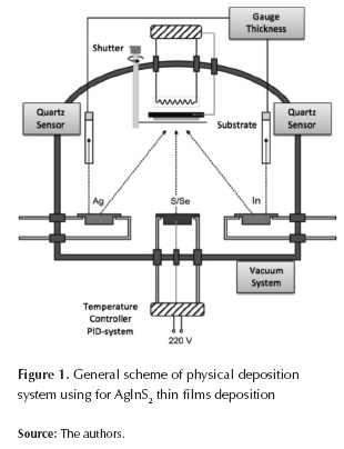
AgInS2 thin films were prepared by co-evaporation from metallic precursor species on glass substrate on an evaporation chamber connected to a vacuum system with pressures around 10-5 Torr, two tungsten crucibles (to evaporate Ag and In respectively), a tantalum effusion cell to evaporate sulfur, and a thickness monitor (Maxtec TM-400) with a quartz crystal to measure the evaporated elements flux. The substrate temperature was controlled with a programmable PID controller (Eurotherm 900C); figure 1 shows general scheme of physical deposition system. AgInS2 thin films deposition was accomplished in two stages. An InxSy layer is grown in the first stage by means of simultaneous evaporation of In and S, keeping the substrate temperature at 300º C. The In flux and S evaporation temperature were kept at 2.5 Å/s and 135°C respectively during the whole stage.
Consecutively, on the second stage, AgInS2 is formed by evaporating Ag (in a chamber filled with sulfur) over a layer of previously grown InxSy (first stage); substrate temperature and Ag flux were 400-600°C and approx. 3 Å/s respectively. AgInS2 films were exposed to a post-deposition thermal annealing in S environment during approx. 1 hour, in order to improve its chemical composition.
In(O,OH)S thin film preparation
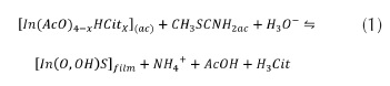
In(O,OH)S layers were deposited using a solution prepared with thioacetamide (Scharlau) (TA) and indium chloride (InCl3) as sources of S2- and In3+ ions respectively; InCl3 was prepared in our laboratory using metallic In (99,9%) and HCl 36% (99.9% Merck). Acetic Acid (99,9% Merck) and Sodium Citrate (Riedel-de Haën) (Cit) were used as complexing agents of In3+ ions. Two substrates were used to grow In(O,OH)S layers: soda lime glass coated with Indium Tin Oxide (ITO) and AgInS2 deposited on soda lime glass; specific experimental conditions are described on Vallejo et al. (2010). The chemical reaction of the film preparation is presented in equation 1, as follows:
Analytical methods
Optical, structural and morphological properties of AgInS2 and In(O,OH)S thin films were studied through transmittance, XRD and AFM measurements carried out with a VIS-IR Oriel spectrophotometer, a Shimadzu 6000 diffractometer with Cu-Kα radiation (λ = 0,15418 nm) source over the diffraction angle 2θ between 20° and 80° and PSI AFM microscope with a scanned area (2 μm×2 μm). Film thickness was determined using a Veeco Dektak 150 surface profiler. AgInS2 conductivity was determined by means of thermoelectric power measurements.
RESULTS AND DISCUSSION
In(O,OH)S thin film growth on AgInS2 layers
CBD process kinetics for In(O,OH)S thin film growth on AgInS2 layers and ITO substrates are presented on figure 2. Results obtained from the trials tend to follow a sigmoidal trend, typical from autocatalytic reactions (O'Brien et al., 1998). Such behavior can be described by means of the Avrami-Erofeev equation (2).
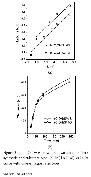
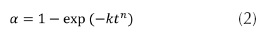
Where α is the fractional decomposition; t the time; k is a rate constant, and n the Avrami exponent which determines the nucleation and growth mode. The equation expresses the rate of formation of the nuclei, in the event when completely random nucleation occurs (Zhai et al., 1007). During the growth process of In(O,OH)S thin film, 3 phases were identified: (1) induction time (start-up of the nucleation process), (2) an initial linear phase, and (3) final saturation phase (figure 2a). Induction time depends mainly on solution temperature, reagents concentration and substrate composition. During the second phase, film thickness increases exponentially with the time, while on the last phase growth rate decreases as reagents concentration decay; normal behaviour of CBD process. Furthermore, it was observed that substrate composition can influence the growth rate of the In(O,OH)S. Kinetic rates are faster when AgInS2 was used as substrate than ITO. CBD growth process is affected by the surface kinetic processes (Froment et al., 1995). Determination of site availability for the formation of nuclei depends on composition and morphology of substrate, particularly the presence of defects as vacancies and interstitials (Ag, In, S) which can facilitate the presence of those sites (Arredondo et al., 2010). If we considered that buffer thin film formation is based on the nucleus generation and succeeding growth (assuming constant temperature during the process), the Avrami-Erofeev equation (3) can be used to calculate the kinetic reaction parameters on different substrates (Zhai, 2007):
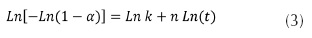
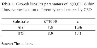
Plotting Ln[-Ln (1-α)] vs Ln (t), the reaction constant (k) and the Avrami exponent (n) can be obtained from the slope and the intercept of the lineal fitting respectively. Figure 2b indicates that substrate type affects growing rate of In(O,OH)S thin films; n value found indicates that both types of substrate consist of the same In(O,OH)S crystals nucleation mechanism because its values are approximately the same (table 1). However, unlike n, k value changes significantly when substrate type varies; this value doubles when AgInS2 absorbent layer is used, indicating that the growth process occurs at a greater rate on AgInS2 than Soda Lime. This phenomenon can be attributed to different nucleation mechanism or the number of sites is different for the generation of nuclei. As a consequence of similar n values in both substrates, nucleation pathway has the same trend, and therefore, AgInS2 presents a greater number of sites for nuclei generation than ITO substrate for In(O,OH)S crystals growing; results explained based on their composition and surface topography (in agreement with reports on Zn(O,OH)S and In(O,OH)S thin films deposition on CuInS2 layers) (Zhai et al., 2007; Vallejo et al., 2010).
Structural characterization
AgInS2 thin films
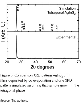
Figure 3 shows XRD spectra of AgInS2 films deposited by co-evaporation; results were analyzed based on the data reported in the JCPDS database for these types of compounds, and performing theoretical simulation of the XRD pattern with PowderCell package. Rietveld method was used for simulation of tetragonal AgInS2-phase; geometry Bragg-Brentano with March-Dollase model was used to find the preferential orientation, and it was found to be (112). The function Pseudo-Voigt 1 was used; the number of iterations was 550 and the final φ factor (shi factor) was 1,5. The described procedure was fundamental to identify the phases present in the samples with a high degree of confidence. It was found that AgInS2 had grown with tetragonal structure. Seven peaks were observed: the highest was observed at 2θ=26,68° corresponding to preferential plane growing (112); other peaks were identified as follows: 2θ=30,4° to plane (200); 2θ=31,96° to plane (004); 2θ=43,55° to plane (220); 2θ=46,62° to plane (204); 2θ=51,80° to plane (312) and 2θ=55,02° to plane (224). These results are in agreement with JCPDS No. 251330. The lattice parameters determined from the X-ray diffraction spectra for AgInS2 films grown with chalcopyrite type tetragonal structure are: a = 5,8980Å and b = 11,1935Å. These results indicate that AgInS2 layer fulfils structural requirements to be used as absorbent layer in thin film solar cells.
In(O,OH),S thin films
Figure 4 shows XRD pattern corresponding to In(O,OH)S thin films deposited on ITO and AgInS2 substrates. Due to its small thickness, crystallinity of In(O,OH)S thin films were very poor; XRD patterns demonstrate that In(O,OH)S layers are polycrystalline. Samples deposited on ITO present just three reflections: the first two at 2θ=33,7º and at 2θ=34,1°, which corresponds to (001) and (200) planes of Indium Oxide Hydroxide (InOOH) (JCPDS # 17-0549), and the third reflection at 2θ=48,37º associated to (2212) plane from tetragonal β-In2S3 phase (JCPDS #25-0390).
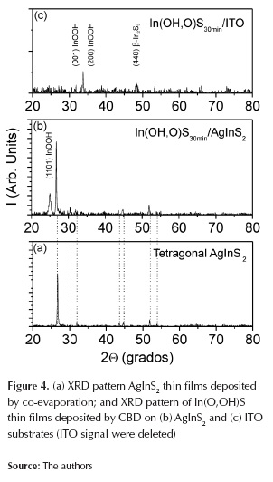
On the other hand, samples deposited on AgInS2 presented one reflection at 2θ=25,7º which corresponds to (110) plane of Indium Oxide Hydroxide (InOOH) (JCPDS # 17-0549). Under reaction conditions, it is possible that during CBD process, a mixture of In2S3, In(OH)3 and In2O3 can be obtained (Larina et al., 2003); however, results reported by other authors on In2S3 thin films structure deposited by CBD, suggesting a mixture of the cubic a and b In2S3 phases (Lokhande et al., 1999; Bayon et al., 2000). The presence of Indium oxide hydroxide and another phases of In2S3 such as g and e have been also reported (Larina et al., 2003, Bayon et al., 2000). Results indicate that buffer layer films deposited on ITO and AgInS2 exhibit polycrystalline structure and might contain a mixture of In2S3 and In(O,OH) phases.
This phenomenon can be explained due to its hydrodynamic of reaction medium because in our case a co-precipitation of another species is possible; due to final composition of buffer layer synthesized by CBD (where different chemical phases are mixed), is common named this material as In(O,OH)S. Along with this, In(O,OH)S thin films deposited by CBD were polycrystalline on both ITO and AgInS2 substrates. These results are important because they indicate that the recipe used allows to obtain polycrystalline thin film independently on the substrate used. To photovoltaic application, it is necessary to obtain a correct junction with electric contact on top cell (ZnO commonly used) for electrical transport and, In(O,OH)S thin films were polycrystalline on AgInS2 substrates, this enhance the junction to electric contact.
Optical characterization
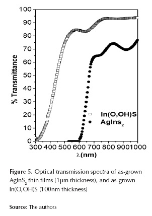
AgInS2 and In(O,OH)S thin films were characterized through spectral transmittance measurements; optical properties of In(O,OH),S were determined from transmission measurements in the range of 300-1000 nm. Figure 5 shows typical transmission spectra of AgInS2 and In(O,OH)S films. In(O,OH)S films deposited on AgInS2 substrate were homogeneous with adequate substrate adherence. In(O,OH)S thin film showed optical transmission of 80-90% in the visible range. High transparency in the visible region indicates absence of adsorbed powdery colloids formed by homogeneous reaction during the film growth. A sharp absorption edge is observed in the visible region, indicating relatively good crystallinity and low defect density near the band edge (Gracia et al., 2005). For AgInS2 thin films, it is observed that transmittance spectra have a sharp absorption edge in the visible region.
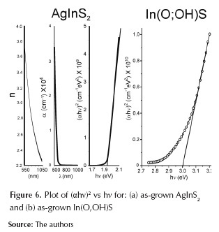
Based on the optical transmission measurements, the square of absorption coefficient (ά2) is plotted as a function of photon energy (hν). Figure 6 shows results of n vs. l, a vs. l and (αhn)2 vs. hn for AgInS2 substrates and buffer layers. Those results were determined based on (Gracia et al., 2005). Figure 6 shows that AgInS2 films have an absorption coefficient a greater than 104 cm-1 and an optical gap Eg of 1,93 eV. These results indicate that AgInS2 thin films have suitable properties for using them as absorber layers in two junction tandem solar cells. In(O,OH)S band gap (3,01eV) was greater than In2S3 bulk band gap (2,4-2,7eV) (Asenjo et al., 2007; Sandoval-Paz et al., 2005); this shift may be due to the CBD technique. The Eg of In(O,OH)S depends on the film's stoichiometry, and it can be found between 2,0 eV and 3,7 eV for In2S3 and In2O3 respectively (Bayon et al., 1998). This result is in agreement with the Eg reported for In(O,OH)S thin films obtained by CBD (Larina et al., 2003; Huang et al., 2001; Yousfi et al., 2000).
In CBD process the co-precipitation of another species is common; in our case, In(OH)3 and In2O3 can be presented in a buffer layer; these compounds could shift the band gap to blue energies; this phenomenon is very favorable because blue response in solar cells enhance system performance. Furthermore, figures 5 and 6 showed that In(O,OH)S thin films presented better optical properties than CdS thin films; this properties allow to use In(O,OH)S thin films as buffer layer on solar cells. Along, differences in band gaps materials are favorable to heterojunction; high band gap values for In(O,OH)S (3,01eV) guarantee that sun radiation on visible range will not be absorbed on the buffer layer but it will be absorbed on AgInS2 (greater than 104 cm−1); this system present typical characteristics to be used in single-junction solar cells and as top cell in a tandem solar cell system.
Morphological characterization
Figure 7 shows AFM images of In(O,OH)S thin films deposited by CBD over AgInS2 layer. The AgInS2-substrate AFM image shows columnar crystals, typical for AgInS2 (1μm thickness) with tetragonal structure; it also shows the effect of In(O,OH)S morphology on thin film thickness; it is clearly seen from AFM images that grain size of In(O,OH)S particles are smaller than grain size of AgInS2 particles (240 nm).
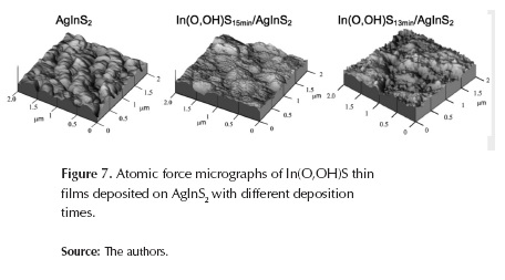
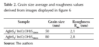
After 15 minutes buffer deposition has started, grain particles of different sizes are distributed randomly throughout the substrate without any crack (figure 7); along, In(O,OH)S thin films grain size and Rms roughness increases significantly when the film thickness increases (table 2). At the initial stage of deposition, many nucleation centers are present on the substrate, and small crystallites are produced; for short time deposition intervals, films with small crystallites are not able to grow into bigger ones, whereas for thicker films the crystallinity of the film crystallites grew bigger. It can also be seen in figure 7 that after 30 minutes of CBD process is possible to cover completely and uniformly the AgInS2 surface. It is a very important requirement for thin films as buffer layer.
Conclusions
By using a system composed of In(O,OH)S/AgInS2 (buffer/absorbent), it was found that In(O,OH)S buffer layers growth on AgInS2 substrates were uniform, adherent and specular. It also presented good macroscopic properties. Furthermore, kinetic studies on deposition of In(O,OH)S over AgInS2 indicated a growth rate variation on the substrate type used. Nucleation process model indicates a significant faster process on AgInS2 than ITO substrates, explained by the differences in composition and topography of the surface substrates. XRD analysis showed that buffer layer films deposited on ITO and CGS exhibited polycrystalline structure with a possible mixture of In2S3 and In(OOH) phases; additionally, it was found that AgInS2 has grown with tetragonal structure at plane (112) as preferential plane. Optical, structural and morphological characterization of the system indicate that In(O,OH)S/AgInS2 layers obtained can be used in single-junction and multiple-junction solar cells.
ACKNOWLEDGEMENTS
This research was supported by Universidad de Medellín, Universidad Nacional de Colombia, Universidad del Atlántico and Universidad Distrital Francisco José de Caldas.
References
Albor, M., Aguilar, J., González, M., & Ortega, C. G. (2007). Photoluminescence studies of chalcopyrite and orthorhombic AgInS2 thin films deposited by spray pyrolysis technique, Thin Solid Films,515(31), 6272-6275. [ Links ]
Arredondo, C., & Gordillo, G. (2010). Photoconductive and electrical transport properties of AgInSe2 thin films prepared by co-evaporation. Physica B: Condensed Matter, 405, 3694-3699. [ Links ]
Arredondo, C., Vallejo, W., Hernández, J., & Gordillo, G. (2012). In(O,OH)S/AgInS2 absorbent layer/buffer layer system for thin film solar cells. 38th IEEE Photovoltaic Specialists Conference (PVSC), 001988-001991. [ Links ]
Asenjo, B. et al. (2007). Study of CuInS2/buffer/ZnO solar cells, with chemically deposited ZnS-In2S3 buffer layers. Thin Solid Films,515(15). 6036-6040. [ Links ]
Barreau, N., Marsillac, S., Albertini, D., & Bernede, J. (2002). Structural, optical and electrical properties of β-In2S3-3xO3x thin films obtained by PVD. Thin Solid Films. 403, 331-334. [ Links ]
Bayon, R. et al. (1989). Preparation of Indium Hydroxy Sulfide Inx(OH)ySz Thin Films by Chemical Bath Deposition. Journal of the Electrochemical Society. 145(8), 2775-2779. [ Links ]
Bayon, R., & Herrero, J. (2000). Structure and morphology of the indium hydroxy sulphide thin films. Applied Surface Science. 58(1-2), 49-57. [ Links ]
Bhattacharya, R., Ramanathan, K., Gedvilas, L., & Keyes, B. (2005). Cu(In,Ga)Se2 thin-film solar cells with ZnS(O,OH), Zn-Cd-S(O,OH), and CdS buffer layers. Journal of Physics and Chemistry of Solids.66(11), 1862-1864. [ Links ]
Contreras, M. et al. (2003). ZnO/ZnS(O,OH)/Cu(In,Ga)Se2/Mo solar cell with 18.6% efficiency. 3rd World Conference on Phorovoltaics Energy Conversion, Osaka. Japan. [ Links ]
Ennaoui, A. et al. (2005). New Chemical Route for the Deposition of ZnS Buffer Layers: Cd-freeCuInS2-based thin film solar cells with efficiencies above 11%. 20th European Photovoltaic Solar Energy Conference. [ Links ]
Froment, M., & Lincot, D. (1995). Phase formation processes in solution at the atomic level: Metal chalcogenide semiconductors. Electrochimica Acta. 40(10). 1293-1303. [ Links ]
Goetzberger, A., Hebling, C., & Schock, H.-W. (2003). Photovoltaic materials, history, status and outlook. Materials Science and Engineering: R: Reports. 40(1), 1-46. [ Links ]
Gracia, M., Rojas, F., & Gordillo, G. (2005). Morphological and optical characterization of SnO2: F thin films deposited by spray pyrolysis. 20th European PV Solar Energy Conference, 1874-1877. [ Links ]
Green, M. et al. (2014). Solar cell efficiency tables (version 43). Progress in Photovoltaics: Research and Applications. 22(1), 1-9. [ Links ]
Hariskos, D., Spiering, S., & Powalla, M. (2005). Buffer layers in Cu(In,Ga)Se2 solar cells and modules. Thin Solid films. 480, 99-109. [ Links ]
Huang, C. et al. (2001). Study of Cd-free buffer layers using Inx(OH,S)y on CIGS solar cells. Solar Energy Materials & Solar Cells.69(2), 131-137. [ Links ]
Larina, L. et al. (2003). Thin film CIGS-based solar cells with an In-based buffer layer fabricated by chemical bath deposition. 3rd World Conference on Photovoltaic Energy and Conversion. 1, 531- 534 [ Links ]
Lee, C. et al. (2012). Design of energy band alignment at the Zn1-xMgxO/Cu(In,Ga)Se2 interface for Cd-free Cu(In,Ga)Se2 solar cells. Physical Chemistry Chemical Physics. 14, 4789-4795. [ Links ]
Loferski, J. et al. (s. d.). RF-sputtered CuInSe2 thin films. 13th IEEE photovoltaic specialists Conference, 190. [ Links ]
Lokhande, C. et al. (1999). Chemical bath deposition of indium sulphide thin films: preparation and characterization. Thin Solid Films, 340(1-2), 18-23. [ Links ]
McEvoy, A., Markvart, T., & Castañer, L. (2013). Solar Cells: Materials, Manufacture and Operation. Second Edition. The Netherlands. Elsevier, 2, 35-45. [ Links ]
Naghavi, N. et al. (2006). From CdS to Zn(S,O,OH): A better understanding of chemical bath deposition parameters and cells properties using electrodeposited CuIn(S,Se)2 and coevaporated Cu(In,Ga)Se2 absorbers. 21st European Photovoltaic Solar Energy Conference, Dresden, 1843. [ Links ]
O'Brien, P., & McAleese, J. (1998). Developing an understanding of the processes controlling the chemical bath deposition of ZnS and CdS. Journal of Materials Chemistry, 8(11), 2309-2314. [ Links ]
Roth, R., Parker, H., & Brower, S. (1973). Synthesis of mercury bismuth sulfide HgBi2S4. Materials Research Bulletin, 8(7), 859-862 [ Links ]
Sandoval Paz, M. et al. (2005). Structural and optical studies on thermal-annealed In2S3 films prepared by the chemical bath deposition technique, Thin Solid Films, 472(1-2), 5-10. [ Links ]
Sankapal, B., Sartale, S., Lokhande, C., & Ennaoui, A. (2004). Chemical synthesis of Cd-free wide band gap materials for solar cells, Solar Energy Materials & Solar Cells. 83(4), 447-458. [ Links ]
Sharma, R. P. (1995). Influence of annealing in vacuum on opto-electronic characteristics of solution grown AgInSe2 films. Indian Journal of Pure & Applied Physics, 33, 711. [ Links ]
Ueno, Y., Kojima, Y., Sugiura, T., & Minoura, H. (1990). Electrodeposition of AgInSe2 films from a sulphate bath. Thin Solid Films. 189(1), 91-101. [ Links ]
Vallejo, W., Clavijo., & J. Gordillo, G. (2010). CGS Based Solar Cells with In2S3 Buffer Layer Deposited by CBD and Coevaporation. Brazilian Journal of Physics, 40(1), 30-37. [ Links ]
Vallejo, W., Hurtado, M., & Gordillo, G. (2010). Kinetic study on Zn(O,OH)S thin films deposited by chemical bath deposition. Electrochimica Acta,55(20), 5610-5616. [ Links ]
Wang, W. et al. (2012). Synthesis of CuInSe2 monodisperse nanoparticles and the nanorings shape evolution via a green solution reaction route. Materials Science in Semiconductor Processing. 15(5), 467-471. [ Links ]
Yoshinory, E., & Hamakawa. N. (1995). Formation and Properties of AgInSe2 Thin Films deposited from Alloy Chunks. Japanese Journal of Applied Physics. 34(1) 3260-3265. [ Links ]
Yousfi, E. et al. (2000). Cadmium-free buffer layers deposited by atomic later epitaxy for copper indium diselenide solar cells, Thin Solid Films, 361, 183-186. [ Links ]
Zhai, R. et al. (2007). Kinetic studies on CaWO4 thin films by chemical bath deposition. Journal of Physics D: Applied Physics. 40, 4039. [ Links ]

