


 English (pdf)
 Article in xml format
 Article references
 Send this article by e-mail
 Cited by SciELO
  Cited by Google
  Similars in
SciELO
Similars in
SciELO  Similars in Google
 Permalink
Introduction
The use of the solar cells technology based on thin films of CdTe and Cu(In,Ga)Se2 (CIGS) has achieved a successful transit to industrial production. However, cadmium is toxic and it requires an effective recycling program, while indium is both sparse and expensive, characteristics which have been considered a great limitation for the large-scale production of modules based on these two technologies in the future (Feltrin & Freundlich, 2008). Cu2ZnSnS4 is emerging as a potential material with several promising properties for inexpensive solar cells made from abundant and non-toxic elements (Khalate, et al., 2018; Yan, et al., 2017).
In 1997, Katagiri, et al. (1997) reported for the first time a solar cell based on CZTS, which had an efficiency of 0.66% and in 2008, they reported conversion efficiencies of 6.7% (Katagiri, et al., 2008). Significant advances were obtained later with solar cells manufactured using CZTS films grown in solution via a hydrazine slurry approach (Winkler, et al., 2014) and other vacuum-based growth techniques have also been successful in fabricating CZTSSe solar cells (Repins, et al., 2012; Yang, et al., 2012). In 2013, a world record for CZTS cell efficiency reaching 12.6% was announced. This achievement was the result of a joint research project of IBM and Tokyo Ohka Kogyo (Wang, et al., 2013) using a device fabricated with a Cu-poor and Zn-rich hydrazine pure solution (Todorov, et al., 2013).
In the present study, we describe a route to grow Cu2ZnSnS4 films free of secondary phases characterized by a high chemical composition homogeneity in the entire volume. To achieve this we built a coaxial evaporation source with an advanced design which allowed growing CZTS films with a chemical composition homogeneity significantly better than those grown by simultaneous evaporation of precursors from separate evaporation sources. These results were verified by XRD and depth profile XPS measurements. We also found that this improved chemical composition homogeneity led to a significant increase of CZTS-based solar cells conversion efficiency.
Materials and methods
The Cu2ZnSnS4 films were deposited using a vacuum-based route including simultaneous evaporation of precursors (Cu, Sn, ZnS) from a cylindrical graphite crucible constituted by two coaxial chambers from where Cu, Sn and ZnS were simultaneously evaporated. Figure 1 shows a diagram of the coaxial evaporation source which was implemented to grow the CZTS films.
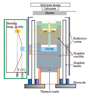
Figure 1 Coaxial evaporation source used to deposit CZTS films by simultaneous evaporation of precursors
The purpose of using a coaxial source was to improve CZTS films chemical composition homogeneity both laterally and in depth which is not possible using laterally separated crucibles to evaporate the precursors. Cu and Sn were evaporated from the same chamber considering that both have similar evaporation temperature while ZnS was evaporated in a separate chamber because it evaporates at a lower temperature. To achieve simultaneous evaporation of Cu, Sn and ZnS, the coaxial evaporation system was built with a special design that allowed to generate a temperature profile such that the temperature of the chamber containing the Cu and Sn precursors was around 1300°C and that of the chamber containing ZnS at around 980°C. The coaxial source was heated by radiation coming from a cylindrical graphite heater and the precursors were co-evaporated in an atmosphere of elemental sulfur evaporated from a Knudsen cell. The CZTS films were deposited on glass substrates or on others coated with a Mo layer using the system as shown in Figure 2a.
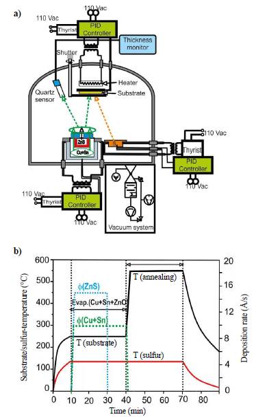
Figure 2 a) Diagram of the system used to deposit Cu2ZnSnS4 films by co-evaporation of Cu, Sn and ZnS in sulfur atmosphere. b) Routine used to grow single phase Cu2ZnSnS4 films
The system was constituted by the following units:
i) A high-vacuum system constituted by a set of mechanical and turbomolecular pumps that allowed obtaining an operation pressure of the order of 2x10⁻⁵ mbar.
ii) An evaporation chamber which included a coaxial evaporation source to simultaneously evaporate Cu, Sn and ZnS, a Knudsen cell to evaporate sulfur, a substrate heating system and a quartz crystal used as a transducer to monitor the flow of the evaporated metallic precursors.
iii) PID controllers to control the temperature of the substrate, the coaxial source, and the Knudsen cell.
iv) A thickness monitor that allowed measuring the thickness and deposition rate of the CZTS sample.
Single phase Cu2ZnSnS4 films were grown using the deposition routine shown in Figure 2b which included simultaneous evaporation of precursors (Cu, Sn, ZnS, S) on a substrate heated to 250°C followed by annealing at 550°C during 40 min. CZTS films with good properties were obtained under the following deposition parameters: ZnS and (Cu+Sn) evaporation rates of 12 Å/s and 15 Å/s, respectively, an evaporated mass ratio (MCu/MSn) of 0.9, and an evaporated mass ratio for MZnS/(MCu+MSn) of 4.
The n+-ZnO layer used as the superior contact of solar cells fabricated with Mo/CZTS/ZnS/n+-ZnO structure were deposited using a route based on the plasma-assisted reactive evaporation method which consists of evaporating Zn in the presence of oxygen to elicit a chemical reaction that gives place to the formation of the ZnO. The system we implemented to grow ZnO thin films by plasma-assisted reactive evaporation and the routine to get ZnO films with adequate optoelectrical properties to be used as window layer of photovoltaic devices are described in Gordillo, et al. (2016). The ZnS film used as a buffer layer was deposited by the chemical bath deposition (CBD) method using a solution containing thiourea (CSN2H4) as the source of HS־ ions, zinc acetate (ZnC4H604 2H20) as the source of Zn2+ ions, sodium citrate (Na3C6H507 2H20) as the complexing agent and ammonia (NH3) for pH adjustment. The following chemical bath composition led to good results: [zinc acetate]=150 mM; [thiourea]=150 mM; [sodium citrate]=30 mM. During the deposition, the bath temperature was kept at 80°C and the solution pH around 10.
The XPS analysis of the CZTS thin films was performed with an X-ray photoelectron spectrometer K-Alpha Thermo Scientific™ using the AlKa radiation (1486.6 eV) for sample excitation. Transmittance measurements were done using a Varian - Cary 5000 spectrophotometer and the film thickness was determined using a Veeco Dektak® 150 surface profiler. The XRD measurements were taken in a Shimadzu-6000 diffractometer.
Results and discussion
Optical and structural characterization of the CZTS films.
The optical properties of the CZTS films were evaluated by determining the absorption coefficient (α) and the energy band gap (E g ) from measurements of the spectral transmit-tance. Both the absorption coefficient and the energy gap were determined using a procedure developed by Swanepoel (1983) to get the optical constants of thin films of amorphous semiconductor materials from theoretical calculations using models that take into account the interference phenomena observed in the transmittance spectrum. The model allows to calculate the refraction index (n) and then the absorption coefficient can be determined by making a curve fitting between a theoretically calculated transmittance curve and the one obtained experimentally. The theoretical transmittance (Tft) as a function of the wavelength λ and the parameters n, a, and the thickness d can be obtained by using the following expression (Swanepoel, 1983):
Where
Solving numerically the equation T Exp - T th = 0, the values of α =((λ) can be obtained.
On the other hand, the optical gap Eg can be determined using the following equation (Pankove, 1971):

where a is the absorption coefficient, A is a constant, E g is the optical band gap and n=1/2 for the direct transition. The optical gap can be determined by extrapolating the linear region of the (ahv) 2 vs the hv curve.
Figure 3 shows the spectral transmittance curve of a typical single phase CZTS film prepared under optimized conditions by co-evaporation and the corresponding curves of α vs λ and (ahv)2 vs hv.
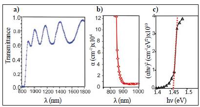
Figure 3 Curves of a) spectral transmittance, b) a vs λ, and c) (ahv)2 vs hv corresponding to a typical single phase CZTS film prepared under optimized conditions
The estimated optical band gap of the CZTS thin films was 1.45 eV, which is in agreement with E g values reported elsewhere (Ennaoui, et al., 2009; Lin, et al., 2011; Tanaka, et al., 2011).
The phase and the crystalline structure in which the CZTS films grew were also studied through XRD measurements. Figure 4 shows the comparison between the XRD pattern of a typical CZTS thin film prepared by co-evaporation from a coaxial source with that of a CZTS film prepared by co-evaporation but using separate crucibles to evaporate the precursors. We observed that the CZTS films prepared with the two methods showed reflections corresponding only to the tetragonal kesterite type Cu2ZnSnS4 phase (AMC cart #99-100-5143). The next section shows the results of the XPS analysis carried out on the CZTS films with which we also verified that the samples grew in the Cu2ZnSnS4 phase.
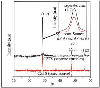
Figure 4 Comparison of the XRD pattern of a typical CZTS film prepared by co-evaporation from a coaxial source with that of a CZTS film deposited using separate crucibles. Inset shows a scan around the (112) reflection.
The scans around the (112) reflection displayed in the inset of Figure 4 show that the full width at the half maximum (FWHM) value corresponding to the CZTS films under study was different indicating that the crystallite size and the microstructure of the CZTS films were affected by the deposition route. Taking into account that the X-ray diffraction peak broadening is due to the instrumental effect as well as to the effect of both the crystallite size (D) and the lattice strain (ε) present in the material, the values of D and ε were estimated using the Williamson-Hall (W-H) equations, which assume that, in addition to the instrumental effect on the X-ray peak broadening, the lattice strain and the crystallite size are the other two independent factors that contribute to the total peak broadening. The contribution of each of these effects was convoluted causing an overall broadening of the diffraction peaks. Before estimating the crystallite size and the lattice strain, the instrumental effect on the broadening βhkl was determined using the following equation (Srinivasan, et al., 2009):
The strain-induced line broadening β
s
, is given by the relation
 and the total peak broadening is represented by the sum of the contributions of crystallite size and strain present in the material. Assuming that the strain present in the material is uniform, the W-H equation for the total peak broadening is given by (Williamson & Hall, 1953):
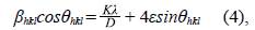
where D is the crystallite size, K is the shape factor (K=0.9), λ is the wavelength of the X-rays (for CuKa radiation), θ hkl is the Bragg diffraction angle (°) and β hkl is the broadening of the hkl diffraction peak measured at half of its maximum intensity (in radians).
A plot taking 4sinθ hkl along X-axis and β hkl cosβ hkl along Y-axis allow to get both the strain present in the material and the crystallite size from the slope and the intercept of the linear fit made to the plot, respectively.
The comparison of the values of the crystallite size and the lattice strain obtained for typical CZTS films prepared by the two mentioned routes is shown in Table 1.
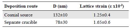
It was observed that the lattice strain ε of CZTS films deposited from the coaxial source was significantly less than that of CZTS films grown by using separate crucibles, which indicates that the CZTS films prepared using a coaxial source grew with improved crystallinity. The results also revealed that the crystallite size of the CZTS samples deposited using the coaxial source were much larger than those deposited from separate crucibles, which favors the electric transport.
XPS analysis. The elemental composition homogeneity in the volume of CZTS film grown by co-evaporation was studied through XPS measurements made at three different depths (sputter time of 1, 6, and 9 minutes, respectively). Figures 5 and 6 show the plots of the high-resolution scans of the Cu2p, Zn2p, Sn3d, and S2p peaks of CZTS thin films deposited from a coaxial source and from separate evaporation crucibles.
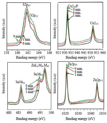
Figure 5 XPS high resolution core level spectra of the Cu2p, Zn2p, Sn3d, and S2p peaks measured at three different depths of typical CZTS thin films prepared by co-evaporation from a coaxial source
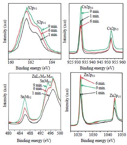
Figure 6 XPS high resolution core level spectra of the Cu2p, Zn2p, Sn3d, and S2p peaks measured at three different depths of typical CZTS thin films prepared by co-evaporation from separate crucibles
It was noted that the XPS scans around the Cu2p, Zn2p, Sn3d, and S2p peaks corresponding to measurements made at the three different depths of the CZTS samples prepared by co-evaporation from a coaxial source (Figure 5), as well as those prepared from separated crucibles (Figure 6), arose at the same binding energies indicating that both types of samples had the same phase and that it did not change throughout the volume. It was also observed that the S2p core level spectrum exhibited two peaks, 2p3/2 and 2p1/2, with binding energies at 161.9 and 162.8 eV and a peak splitting of 0.9 eV, while the Sn3d core level spectrum showed two peaks, Sn3d5/2 and Sn3d3/2, at 486.4 and 495 eV with a separation of 8.6 eV, while the Cu2p core level spectrum exhibited binding energies for the Cu2p3/2 and Cu2p1/2 peaks at 932.7 and 952.3 eV and a peak splitting of 19.6 eV while the Zn2p core level spectrum peaks Zn2p3/2 and Zn2p1/2 were visible at the binding energies of 1021.8 and 1044.6 eV with a peak separation of 22.8 eV. These results allowed us to conclude that in both types of samples copper was in the +1 oxidation state, Zn in the +2 oxidation state, and S in the -2 oxidation state, which also confirmed the valence (IV) for Sn. Similar results have been reported in other studies (Riha, et al., 2009; Xu, et al., 2012).
Results in Figures 5 and 6 also show that the peak area of the core level spectra for elements Cu, Zn, Sn, and S, measured at different depths of the CZTS films co-evaporated from a coaxial source differed very little from each other indicating that the chemical composition of this type of samples was homogeneous; on the contrary, the samples prepared by co-evaporation from separate evaporation crucibles exhibited inhomogeneity in their chemical composition throughout the entire volume.
Cu2ZnSnS4-solar cells. Solar cells with the structure Mo/Cu2ZnSnS4/ ZnS/n+-ZnO were fabricated using typically a 0.6 μm thick Mo layer, a 3.0 μπι thick CZTS film, a 50 nm thick ZnS buffer layer deposited by CBD, and a 0.8 μm thick n+-ZnO layer and its J-V characteristic was measured under AM 1.5 irradiance (100 mW/cm2). In Figure 7 we compared the J-V curve of the best solar cell fabricated using a CZTS layer deposited from a coaxial source with that of a cell fabricated using a CZTS layer deposited using separate evaporation crucibles and in Table 2 we listed the corresponding performance parameters (open-circuit voltage (VOC), short-circuit current density (Jsc), fill factor (FF) and conversion efficiency (η)).
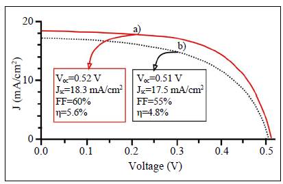
Figure 7 J-V curves of the best solar cells fabricated using a CZTS absorber layer a) deposited from a coaxial source and b) from separate evaporation crucibles
Table 2 Comparison of the performance parameters of solar cells fabricated using CZTS layers deposited by co-evaporation from a coaxial source with that of devices fabricated using a CZTS layer deposited by co-evaporation from separate evaporation crucibles
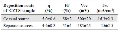
From the data in Table 2, it is observed that the low efficiency of CZTS-based cells was mainly caused by poor FF and low short circuit current. Taking into account that the FF depends on the diode quality factor β, as well as on its series resistance, the low values of FF could be partly attributed to the high values of the series resistance of the cells. On the other hand, considering that the diode quality factor is affected by the recombination through the trap centers inside the depletion region (Mialhe, et al., 1986), it can be assumed that an additional loss of FF may be related to the presence of recombination centers in the depletion layer of the device, probably induced by structural and intrinsic defects (vacancies, anti-site defects, etc.).
The low values of short circuit current exhibited by the studied solar cells suggest a low collection of the photo-generated carriers, which could be attributed to factors such as, small minority carrier diffusion length associated with small grain size values of the CZTS layer and also with high densities of trap states. The high interface state recombination may be another factor contributing to losses of the short circuit current.
The best efficiency obtained in this work was 5.6%; however, bearing in mind that these are just preliminary results, the performance of the device could be improved by optimizing the growth parameters of the different layers that constitute the device and improving the grain size of the CZTS films through the optimization of the post-deposition annealing.
Conclusions
Single phase CZTS thin films with improved chemical composition homogeneity were grown by co-evaporation of precursors from a coaxial evaporation source built with an advanced design. XRD and XPS analyses revealed that the oxidation states of the constituent elements of the CZTS films corresponded to the Cu2ZnSnS4 phase. On the other hand, we found that the CZTS films presented a high absorption coefficient and an optical gap of 1.45 eV indicating that they are suitable to be used as absorber layer in solar cells.
The applicability of the CZTS films grown by co-evaporation of precursor for solar cells was demonstrated and its performance was significantly enhanced by improving the homogeneity of the chemical composition of the CZTS layer. Efficiencies of 5.6% were achieved with solar cells fabricated with the structure Mo/Cu2ZnSnS4/ZnS/n+-ZnO.

