


 English (pdf)
 Article in xml format
 Article references
 Send this article by e-mail
 Cited by SciELO
  Cited by Google
  Similars in
SciELO
Similars in
SciELO  Similars in Google
 Permalink
INTRODUCTION
The energy we use in our planet comes mainly from non-renewable sources such as oil, coal, natural gas and only 10.4 % comes from renewable energy sources of last genera tion. Taking into account all renewable energies, the photovoltaic solar is the one that has had more growth of installation in the last years, more than those coming from the coal and gas together. Research in solar cells has achieved the obtaining of high efficiencies among which 26.1 % are achieved with silicon cells, 22.1 % with CdTe, and 27.8 % with GaAs [1]. Among the diverse materials studied to develop solar cells with thin film technology stand out those based on Cu(In,Ga)Se2 (CIGS) and CuInSe2 (CIS), because the maximum efficiency obtained until now in solar cells of this technology on rigid substrates is 23.35 % [2, 3] and 20.8 % on flexible substrates [4].
The functioning of a solar cell is determined by some physical variables that when established can be obtained information about what may be affecting the performance of the photovoltaic device. This information allows to study strategies that would enable to improve the efficiency of the device. In the literature, several methods of estimation of parameters of these systems are presented, however, most of the processes to obtain the parameters of photovoltaic systems are only theoretical and have been focused on applying them to commercial modules mainly. Additionally, it presents a profusion of methods related to heuristics [5, 6] and recently theoretical hybrid versions of optimi zation algorithms have been proposed to optimize the solar cell parameters [7]. This work is novel because from experimental measurements of solar cells manufactured in our laboratory their electrical parameters are determined using two theoretical models of diodes, these simulation models are used as a tool that allowed us to analyze the factors that from the physical point of view affect the performance of the cells. In this way, implementing an optimization process using the generalized reduced gradient were determined the photogenerated current, the dark current of the diode, the series resistance, the parallel resistance and the ideality factors of diode of CIS-based solar cells prepared in the laboratory.
1. METHODOLOGY
1. 1. Fabrication and characterization of the solar cell
Solar cells were fabricated in the laboratory using thin film technology with Mo/ CIS/CdS/n+-ZnO structure, Figure 1 shows in schematically the cross-section of a typically prepared solar cell. The bottom contact of the cell is a thin film of Mo with a 1 mm of thickness deposited by the method sputtering DC magnetron, the synthesis parameters were Argon pressure = 1.5 x10⁻² mbar, current = 200 mA, voltage = 280 V, deposition time = 25 min. The absorbent layer of CIS with 3 mm thickness was deposited on the Mo layer in a two-stage process: in the first stage was evaporated the precursor layer of Cu at 1100 °C on the Mo at room temperature for 5 minutes, in the second stage were evaporated simultaneously In2Se3 at 880 °C and Se at 230 °C for 10 minutes keeping the substrate temperature at 550 °C. On the absorbent layer the Cd buffer layer was deposited with a thickness of 70 nm by the Chemical Bath Deposition (CBD) method. Subsequently, the highly transparent n+-ZnO of 1 ^m thickness was deposited as n-type layer by the reactive evaporation method. Finally, a grid of Ag is deposited by evaporation. The solar cells were deposited on a soda-lime glass substrate with an active area of 24 mm2.
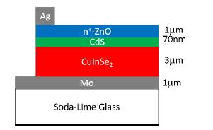
Source: own elaboration.
Figure 1 Diagram of a typical solar cell prepared with structure Mo/CIS/CdS/n+-ZnO
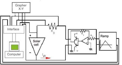
The solar cells prepared were characterized by measuring the I-V curve to determine its main operating parameters. In Figure 2 are showed schematically the equipment used to carry out the measurements of the I-V curve of solar cells.
Source: own elaboration.
Figure 2 Diagram of the system used to carry out measurements of the I-V curve of solar cells
The equipment consists of the following elements:
Interface: it allows the acquisition of data, controls the functioning of the system, calculates the parameters of the solar cell (Isc, Voc, n), performs the graph and theoretically calculates I vs V.
Ramp: generates the bias voltage of the solar cell between -0.5 V and 0.7 V approximately. The voltage ramp is generated using the LabView software, it is applied to the cell through a power stage.
Computer: it controls the process, generates the voltage ramp, stores and processes the data obtained.
Grapher X-Y: allows to graph the I-V curve at the same time as the corresponding data is captured on the computer.
R0: it is used to determine the current generated by the solar cell by measuring the potential drop in it (V = IR0).
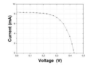
Figure 3 shows the I-V characteristic curve obtained experimentally for the best solar cell prepared using irradiation of 100 mW/cm2, the experimental uncertainty in the voltage measurement was ±2.5 mV and in the current ±0.05 mA. The measurements of the I-V curve provided information about the output parameters that characterize the functioning of the solar cell fabricated, which are: open circuit voltage (Voc)=0.43 V, short-circuit current density (Jsc)= 34 mA/cm2, fill factor (FF)= 0.63 and efficiency (n)=9.2 %. This I-V characteristic curve was also used to estimate the electrical parameters of the cell by means of the single and double diode models as can be seen in the next section.
1.2 Parameter estimation
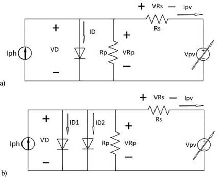
For the purpose of understanding the electrical behavior of a solar cell, it was appropriate to use equivalent circuit models [8, 9], (a) and (b) with one and two diodes respectively, as shown in Figure 4. Each circuit model is composed of two resistances: one series resistance Rs which models losses that depend on the resistivity in the volume of the active semiconductor and the metallic contact [10], and a parallel resistance Rp which is related to the current losses at the edges of the cell and the homogeneities on the surface of the cell [11]. In order to the conversion efficiency to be high, Rs and Rp must be small and high respectively. The electric current generated by the solar cell exposed to the sunlight is modeled by the current source Iph in the electric circuit.
In Figure 4a, single diode model has some inaccuracies at low irradiance levels and the recombination current is neglected. In Figure 4b, double diode model is used because is more precise due to the fact that it takes into account the current due to junction recombination [12], but this model needs more parameters compared with single diode model.
Source: own elaboration.
Figure 4 a) Single and b) Double diode models to a solar cell with a connected variable load
Parameter estimation is carried out by optimizing the objective function based on the square mean error method to determine the optimal parameter estimates, all this subjected to constraints obtained from the respective model.
The first constraint for the single diode model is obtained using the current Kirchhoff law to the circuit of the Figure 4a, equation (1):
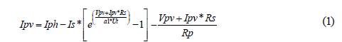
Where Ipv is the photovoltaic current, Is is the dark current of the diode, Vpv the photovoltaic voltage and, finally, Rp and Rs as they were previously defined.
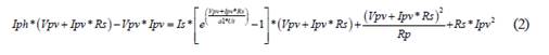
The second constraint for the single diode model is obtained using the power conservation law, where the algebraic sum must be equal to cero, equation (2):
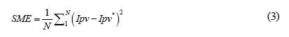
The mathematical equation (3) describes the objective function that correspond to the Square Mean Error (SME) defined to the measured and estimated currents, the latter marked with an asterisk (*).
The first constraint to the optimization problem taking the double diode model, Figure 4b, correspond to the current Kirchhoff law, equation (4):
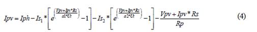
The second constraint to the optimization problem taking the double diode model, Figure 4b, correspond to the power conservation law, equation (5):

The objective function is the same used in the optimization processes for a single diode circuit, equation (3).
On the other hand, the information obtained experimentally is taken from the curve I-V of Figure 3, whose parameters are: Voc = 0.43V, Jsc = 34 mA/cm2, FF = 0.63 and n = 9.2%.
The modeling process was carried out by implementing the model in GAMS software [13] and the optimization process was carried out using the CONOPT3 solver [14]. The algorithm used is shown in Figure 5.
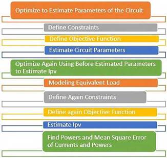
The steps involved during the modeling and optimization process are detailed below:
Obtain the experimental data and the circuits to use, Figures 3 and 4.
Construct all the system constraints. Single diode model, equations (1) and [2]. Double diode model, equations (4) and [5]. Here the variables are the parameters of the circuits.
Construct the objective function, equation (3) for both circuit models.
Obtain the optimal parameters of the circuits. Tables 1 and 2.
Model a load connected to the solar cell using a variable voltage source, Figure 4. Voltage values were obtained in Figure 3.
Construct the objective function, equation (3) for both circuit models.
Construct all the system constraints. Single diode model, equations (1) and [2]. Double diode model, equations (4) and [5]. Here the variables are the currents of the circuits.
Obtain the square mean error of currents in order to make comparisons.
2. RESULTS AND DISCUSSION
From the experimental data of the IV curve shown in Figure 3 and the optimization process previously described, the electrical parameters characteristic of the studied solar cell were obtained, that is, a thin film solar cell with Mo/CIS/CdS/n+-ZnO structure. The results for each model of the analyzed diode are presented below.
2.1 Single diode model
The parameters obtained with the single diode model are presented in Table 1 and Figure 6 shows the comparison between the characteristic IV curve obtained from the algorithm described above and the experimental data.
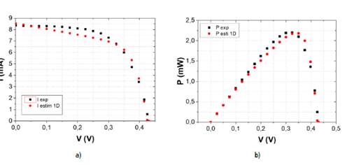
Figure 6 Comparison between a) IV and b) PV curves measured from experimental data and estimated parameters in thin film solar cell with structure Mo/CIS/CdS/n+-ZnO
Table 1 Estimated values from single diode model.
| PARAMETER | VALUE OBTAINED |
|---|---|
| photocurrent Iph (A) | 0.0086 |
| Dark current Is (nA) | 1.97820 |
| Series Resistance Rs (Q) | 1.1898 |
| Shunt resistance Rp (Q) | 200.1304 |
| Diode ideality factor a1 | 1.0972 |
Source: own elaboration.
Source: own elaboration. It was observed that the adjustment resulting from this model does not allow a good ap proximation to the experimental IV and PVs curves due mainly to the shunt resistance (Rp) being low (of the order of200 Q), that allow current leakage in the solar cell. The maximum power obtained from the experimentally data was 2.2105 mW, this value was used for both models of the diode in the estimation of the parameters from the measurements.
The mean squared error for the single diode model was 0.1437 mA for the current and 0.0110 mW for the power. In the case of the mean square error for the current measure ment, the value of 1.67 % is outside the range of the laboratory measurement accuracy class device, labelled 0.5.
2.2. Double diode model and physical analysis of the two models
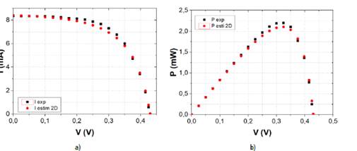
Table 2 presents the parameters for the double diode model. Figure 7 shows the com parisons of the IV and PV curves using the double diode model with the experimental results and the estimation of parameters.
Source: own elaboration.
Figure 7 Comparison between a) IV and b) PV curves measured from experimental data and estimated parameters in thin film solar cell with structure Mo/CIS/CdS/n+-ZnO
Table 2 Estimated values from double diode model.
| Parameter | Value obtained |
|---|---|
| Photocurrent Iph (A) | 0.0084 |
| Dark current of diode1 Is1 (A) | 2.378200E-10 |
| Dark current of diode 2 Is2 (A) | 4.9208337E-5 |
| Series Resistance Rs (Q) | 0.1 |
| Shunt Resistance Rp (Q) | 2352.9857 |
| Diode ideality 1 factor a1 | 1.0278 |
| Diode ideality 2 factor a2 | 3.5017 |
Source: own elaboration.
For the double diode simulation model, the mean square error of the current and power were equal to 0.0361 mA and 0.0030 mW respectively. In the case of the mean square error for the current measurement, the value of 0.43 % is smaller the range of the laboratory measurement accuracy class device, labelled 0.5. This model allowed a better fit to the experimental I-V curve of the cell than the single diode model.
In both models (single and double diode), the photocurrent value remains appro ximately constant due to the source of photocurrent generation being kept between 8.4 and 8.6 mA. This source simulates the current generated when sunlight is absorbed in the solar cell.
The dark current Is of the single diode model decreased from 1.9782 x10⁻⁹ to 2.3782x10⁻¹⁰ A in the double diode model, which indicates a low dark current, suitable for a good operation of the solar cell. The ideality factor of the diode of both models results closer to 1 and changed from 1.0972 in the single diode model to 1.0278 in the double diode model, which indicates that the manufacturing process of the p-n junction of the solar cell presents fewer physical defects in the double diode model and the simulation of experimental data is closer to reality. In the last diode model the value of the series resistance decreased approximately one order of magnitude from 1.1898 Q to 0.1 Q and the shunt resistance increased from 200.13 Q to 2352.98 Q, this provided a better fit to the IV and PV curves. Even though the other parameters influence the better adjustment of the curves, it was observed that the greatest effect is under the influence of series and shunt resistance, this is in accordance with other investi gations [15, 16].
Although the series resistance is low, it influences the experimentally obtained fill factor of 0.63. The value of the shunt resistance is not great enough to give a good efficient behavior probably due to the interdiffusion across elements that make up the layers of the solar cell such as the Cu towards the surface of the cell and migration of other elements [17]. The adjustment of the IV and PV curves obtained with the double diode model also indicates that the solar cell produced presented some interfacial states at the p-n junction, which can generate charge recombination processes at the interface. The study allows the identification of the factors that affect the efficiency of the solar cells prepared in the laboratory to improve the experimental preparation conditions.
3. CONCLUSIONS
From the experimental curve I-V, the electrical parameters of a solar cell were estimated using the single and double diode models. These models were based on the charac teristic circuits of the solar cell and by means of the optimization process using the generalized gradient method, the variables of the models were obtained, which refers to an innovative tool to determine with enough approximation the physical variables of a solar cell. The single diode model did not allow a good fit to the IV experimental curve, while the double diode model was closer to the curve allowing physical variables to be established. It was evidenced that in the manufactured solar cells, some energy states can be presented in the p-n junction interface, diffusion of elements between layers, electrical resistances in the transparent layer and in the electrical contacts that affect its operation avoiding a higher efficiency.
The double diode model presented a minor error in the measurement of the current, compared with the single diode model. Comparing the errors obtained in the measurements of current with respect to the estimates, it can be observed that for the equivalent circuit of single diode model, the estimated error is outside the range of the class of equipment used in laboratory measurements, due to it being greater than 0.5. On the other hand, for the equivalent circuit that has two diodes, the estimated error is within the range of the class of equipment used in laboratory measurements, because it is less than 0.5.

