


Services on Demand
Journal
Article
 English (pdf)
 Article in xml format
 Article references
 Send this article by e-mail
Indicators
-
 Cited by SciELO
 -
 Access statistics
Related links
-
 Cited by Google
 -
 Similars in
SciELO
Similars in
SciELO -
 Similars in Google
Share

 Permalink
Tecciencia
Print version ISSN 1909-3667
Tecciencia vol.10 no.18 Bogotá Jan./June 2015
https://doi.org/10.18180/tecciencia.2015.18.6
DOI: http://dx.doi.org/10.18180/tecciencia.2015.18.6
Development board based on the TMS320F28335 DSP for applications of power electronics
Placa de desarrollo basado en TMS320F28335 DSP para aplicaciones de electrónica de potencia
Julian Saavedra1, Jonathan Firacaitve2, Cesar Trujillo3
1 Universidad Distrital Francisco Jose de Caldas, Bogotá, Colombia, ifsaavedram@correo.udistrital.edu.co
2 Universidad Distrital Francisco José de Caldas, Bogotá, Colombia, jafiracative@corre.udistrital.edu.co
3 Universidad Distrital Francisco José de Caldas, Bogotá, Colombia, cltrujillo@udistrital.edu.co
* Corresponding Author. E-mail: jfsaavedram@correo.udistrital.edu.co Tel: + 57 1 3239300 ext 1510
How to cite: Saavedra, J.; Firacaitve, J.; Trujillo, C. Development board based on the TMS320F28335 DSP for applications of power electronics, TECCIENCIA, Vol. 7 No. 18., 36-44, 2015, DOI: http: http://dx.doi.org/10.18180/tecciencia.2015.18.6
Received: 11 Aug 2014 Accepted: 14 May 2015 Available Online: 29 May 2015
Abstract
This paper presents the design of a special purpose development board for power applications based on the digital signal processor (DSP) TMS320F28335. We also propose some considerations for the design of any four-layer printed circuit line with international recommendations to counteract the EMI (electromagnetic interference) and increase the EMC (electromagnetic compatibility). Additionally, the main features of each module on the board and their respective conditioning circuits designed are presented in order for the development board to be useful for any application of power electronics as motor control, switching power supplies, LED lighting, communications through the electric network, etc. Finally, a test protocol to verify the performance of the card and the comparison between the final cost per unit and similar cards on the market were performed.
Key Words: anti-aliasing filter, electromagnetic interference, multilayer printed circuit board, signal conditioning, sensitivity.
Resumen
En el presente artículo se presenta el diseño de una tarjeta de desarrollo de propósito específico en aplicaciones de potencia con base en el procesador digital de señales (DSP) TMS320F28335. Se proponen adernas unas consideraciones para el diseño de cualquier circuito impreso de cuatro capas acordes con las recomendaciones internacionales para contrarrestar los efectos de interferencia electromagnética (EMI) y aumentar la compatibilidad electromagnética (EMC). Como factor adicional se presentan las principales características de cada modulo en la placa y sus respetivos circuitos de acondicionamiento, esto con el fin de que la placa de desarrollo sea útil para cualquier aplicación de electrónica potencia como control de motores, fuentes conmutadas, iluminación LED, comunicaciones a través de la red eléctrica, etc. A continuación, se realizó un protocolo de pruebas para verificar el funcionamiento de la tarjeta y la comparación entre el costo final por unidad y las tarjetas similares presentes en el mercado. Finalmente, se presentan las conclusiones en donde se resalta que la tarjeta implementada cumple con las características adecuadas para operar en el desarrollo de prototipos electrónicos de potencia a nivel de innovación y/o investigación.
Palabras clave: Acondicionamiento de señales, circuito impreso multicapa, filtros antialiasing, interferencias electromagnéticas, sensibilidad.
1. Introduction
Today, renewable energies have gained a lot of importance in the sustainable development of nations. Worldwide energy consumption of renewable sources exceeds 25% and is expected to increase by 50% at the middle of this century. Societies are increasingly consuming such resources in order to achieve energy coverage for the entire population. The wide array of renewable energy sources includes solar, wind, geothermal, biomass, tidal, and wave power, among others [1].
Thus, the Investigation Group LIFAE (the Spanish acronym for Research Laboratory of Alternative Sources of Energy) of the Universidad Distrital Francisco José de Caldas in Bogotá, Colombia investigates such issues, specifically photovoltaic systems, solar radiation and ambient temperature characterization, stand-alone and interconnected systems, and their respective applications. These investigations have been based on energy processing, understood as the transformation of renewable energies into electricity suitable for isolated loads or grid feeding and associated power electronics (topologies of DC-to-DC converters, inverters, Voltage-Source Converters (VSC) and High-Voltage Direct Current (HVDC) based on VSC) [2].
To accomplish the above, computer systems with high processing capabilities are required in order to properly develop control algorithms and perform energy management. Hence, the need arises for low-cost devices which operate at high frequencies, have low consumption, the capacity for signal processing in real time, a high level of integration, high resolution and are adaptable to specific applications of power electronics, which perform the processing of energy [3].
Consequently, in this study we seek to analyze a purpose board specific for applications in power electronics in order to support the DSP, which is an electronic device that fully meets the above characteristics. Furthermore, we expect the development of a series of circuits which allow for peripherals to adapt to the function required, as well as the adaptation of analog to digital signals, the modification of the Pulse-Width Modulators (PWM), the conditioning of general-purpose input/output signals, and the implementation and operation of different communication systems (I2C, SPI, etc.) for the transmission of signals of interest such as the signals transmitted to the Digital-to-Analog Converter (DAC), among others.
2. Methods and materials
2.1. DSP Selection
The wide variety of specialized digital signal processors in different electric and electronic applications, require taking into account specific criteria for the selection of DSP, such as arithmetic format, data bus, speed of execution and transmission, memory size, number of PWM channels, sample rate and resolution of the analog-to-digital converter. Thus, the selection of specific DSP provides adequate performance to the system in which the processor is going to be included [4].
The DSP was selected considering it would have a floating-point format. It is ideal for applications requiring flexibility, high dynamic range and accuracy. A second parameter that was considered was the operation frequency. In addition, the amount and variety of peripherals were also taken into account. In this way, and based on the above, it was established that the Texas Instrument processor TMS320F28335 was the processor which meets the criteria at an appropriate cost.
2.2. Digital Signal Processor TMS320F28335
The TMS320F28335 is a 32-bit floating-point DSP belonging to the sub-family of Texas Instruments C2000 Delfino, which combines the versatility of a general-purpose microcontroller with the high precision and performance of a digital signal processor. It is made of technology CMOS, can operate at a frequency of 150 MHz and has modified Harvard architecture. From a power electronics perspective, the most important module is the pulse width modulation. There are six of these modules, where each consists of two complementary outputs containing a common 16-bit counter. Each time a sample parallel is taken, a channel of each module can work at a higher resolution (24 bits).
Furthermore, the DPS has 16 channels for analog-to-digital converter module with 12-bit resolution at a fast conversion speed up to 80 ns. The improved quadrature encoder module is considerably useful for obtaining information on the position, direction and speed of a rotary machine. It has three 32-bit timers and has a varied group of protocols in the communication port [5]: Serial Peripheral Interface (SPI), Inter-Integrated Circuit (IIC), Controller area Network (CAN), Serial Communication Interface (SCI).
2.3. Modules adapted to the development board
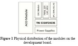
The development board is divided into four groups, as shown in Figure 1. In the ADC module there are circuits with analog signals and it consists of anti-aliasing filters, conditioners, circuits of protection and overvoltage, and analog-to-digital converter (ADC). The module named in the figure as "PWM, QUEP. CAP, GPIO" goes to the digital part consisting of PWM generator, module of capture external events (CAP), incremental rotary encoder interface (QEP) and module to the General-Purpose Input/Output signals (GPIO). Similarly, the module appearing as "SPI, CAN, SCI, IIC" consists of the communication port conformed by the modules (SPI, IIC, SCI, CAN). In addition, there is a DAC module and a module including the polarization sources for both the digital part and analog part.
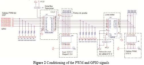
The signal generator module PWM has 12 independent channels. Signal conditioning was implemented through the level shifter CD4504b IC (Integrated Circuit), which allows for three (3) different output voltage values (3.3, 5, 15) V. It includes four (4) buttons for handling external interrupts, which are responsible for forcing the output level of the PWM signal to a level predefined by software. The GPIO module was conditioning by the IC of the 74LVC245ADWR bidirectional data Buffer. This module has 27 shared inputs/outputs and six (6) independent inputs/outputs with the output voltage level conditioned as the PWM module, as shown in Figure 2.
The eCap is exclusively dedicated to the accurate capture of external events. It presents six (6) channels that can perform as an auxiliary PWM signal generator.
The eOEP module was likewise adapted as an interface between an incremental rotary encoder and the DSP. It has a Quadrature Decoder Unit (QDU), a Position Counter and Control Unit (PCCU) and a Unit time base for speed/frequency Measurement (UTIME).
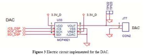
Because the DSP does not have an analog-to-digital converter, the SPI for the exchange of data between the DAC and the DSP was defined, since it offers a higher transmission speed than the IIC and the tuple data is 16 bits. Figure 3 shows the electric circuit implemented for such convertor. DAC module has a 12-bit resolution channel and an output signal between (3-0) V, conditioned to the board by the IC MCP 4921.
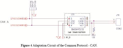
The CAN protocol is based on the Carrier Sense Multiple Access model with a transmission rate up to 1 Mbps and a range of 40m. It discerns between temporary errors and permanent failures of nodes. It is adapted to the ISO 11898 Standard by the IC SN65HVD232 CAN transceiver, as shown in Figure 4.
The SCI is an asynchronous serial communication protocol with double buffer for transmission and reception functions. It is adapted to IC SN75179B differential driver and receiver pair, and is ideal for applications with balanced transmission lines in the RS-485 and RS-422 standards.
The ICC Module has a transmission rate of between 10 kbps and 400 kbps. It is compatible with the Semiconductors IIC-bus v2.1 and is decoupled through the IC ADuM1250.
The conditioning of the peripheral SPI was performed through the integrated circuit ADuM1401 of four separate and isolated channels, which are based on Analog Devices, Inc., iCoupler® technology, as seen in Figure 5.
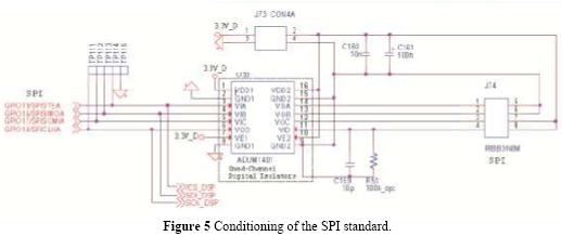
This device is characterized by its low power consumption (a tenth of the conventional optocouplers, approximately) and ease of operation. It was created to be used in applications with SPI interface for converting data with a transmission rate up to 90 Mbps.
2.4. Anti-aliasing filter - ADC Module
Signals acquisition was made by the analog-to-digital converter, which performs a sampling that must satisfy the condition of the Nyquist-Shannon sampling theorem. In case this parameter fails to be met, a phenomenon known as Anti-aliasing occurs [6]. Therefore, by means of a low-pass filter, any signal outside the range of interest (sampled signal) gets eliminated and the presence of such phenomenon avoided.
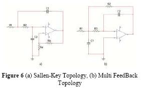
Topology selection focused on the searching of the one involving less active elements, thereby decreasing the cost of the filters and the space on the printed circuit board (PCB).
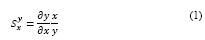
Of the main topologies [7] [8], Sallen-Key Topology (Figure 6a) and Multi FeedBack (MFB) Topology (Figure 6b) both contain a single operational amplifier for a second order filter. Among these two, a sensitivity analysis was performed [7], defined in Equation 1 where y represents parameters that mathematically model the filter and x represents the values of resistors and capacitors conforming the filter, thus finding the topology representing less percentage changes in the quality factor Q and in the natural frequency of the filter ω0, according to the percentage changes in the market values of the passive elements composing it. Topology to be selected was based on the sensitivity calculations, the resistance for frequencies and the lower value of the synthesis of the sensitivities.
2.5. PCB Design
Currently available technology has led to have circuits with a higher level of integration, considerably reducing the sizes of the PCB and thus increasing the capacity of interfering one signal into another and, in general, adverse electrical factors affecting signal integrity.
PCB design for the implementation of the board and in general for any multilayer PCB, was based on the following considerations so that the effects of EMI and EMC counteract [9] [10] [11] [12] [13] [14]:
- The outward and return path of a signal should be close enough so that the inductance of the circuit is reduced and thus the magnetic field flux generated.
- The larger the area of the conductor is the reactance substantially decreases, thus controlling the effects of electric and magnetic fields.
- Creating return planes on the signal layer helps to substantially lower the inductance of the paths and therefore the total inductance of the PCB. This plane catches and drains the radiation generated by the signals interacting in the printed circuit board
- If the PCB presents return planes in the outer layers, must be verified that there are not small isolated copper areas (island) as these behave likely as microstrip antennas, susceptible to radiate electromagnetic fields of adjacent signals. Moreover, if there are large copper segments that are not connected to the ground plane on the return plane, these must be grounded via routes known as "stitching vias".
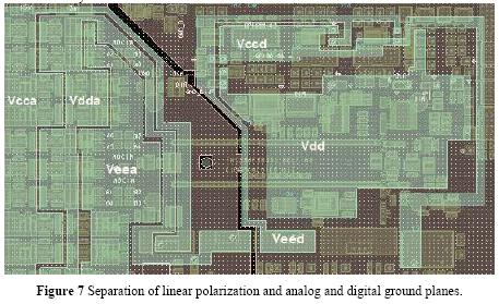
- Linear polarization and analog and digital ground planes must be separated, as shown in Figure 7.
- Location of the parts having connections in common should be as close as possible and the copper traces short and straight. In digital circuits, if the above condition cannot be met, parts that are functionally related must kept close or the pieces with clock signals at high frequencies and very short rising edges must be grouped. Thus, the size of the paths carrying these signals can be minimized.
- In accordance with the IPC 2251, paths greater than λ/15 length, must be designed according to the transmission lines theory.
- In mixed PBC, meaning those composed of analog, digital and power circuits, these must be distributed in different areas and only if necessary, join them into a single point. If along the PCB different frequency bands are presented, components whose signals have low spectral components should be located inside the plate. Moreover, components with higher frequency signals must be located in the periphery of the PCB, previous to the connectors.
- Likewise, the following parameter for the distribution layers was considered: signal layers must be as close as possible to ground planes in order for EMI to reduce.
- Linear polarization must be adjacent to ground/return planes for adding capacitances between planes, which helps to reduce polarization noise and electromagnetic radiation.
For the separation of copper paths, the 3W Rule is suggested, which states the spacing distance as three times the width of the path, between traces centers.
- Avoid 90 degrees angles on paths carrying signals in high frequency band or higher, as these increases the width of the track with a factor of 1.414, thus affecting the characteristic impedance at the corners of the paths. Thereby, changes in the trajectory greater than 45 degrees are not recommended.
- The use of decoupling capacitors helps filtrating the radiofrequency noise present in the signal power of integrated circuits. To use two or three different types of capacitors (tantalum, ceramic, electrolytic, etc.) with values decline for decades from 0.1 nF is recommended.
3. Results
3.1. Topology definition for the antialiasing filter
Table 1 (were recommendation [9] was also followed to decrease sensitivity in the Sallen-Key topology regarding passive elements), were obtained. The statements in this table are given by the combination of the nominal values of the passive elements, which in turn, are in function of the frequency response required to implement. Such response is established towards minimizing the distortion in phase and magnitude to the signals to be sampled [16] [17] [18] [19]
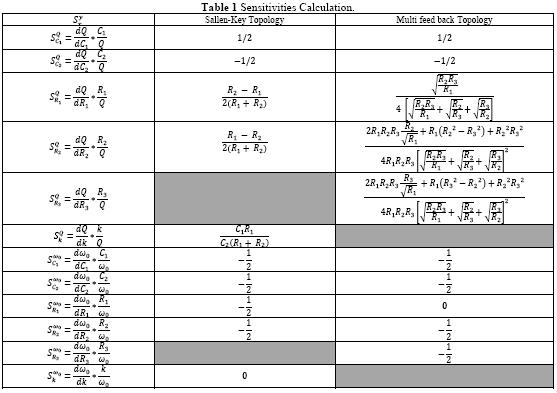
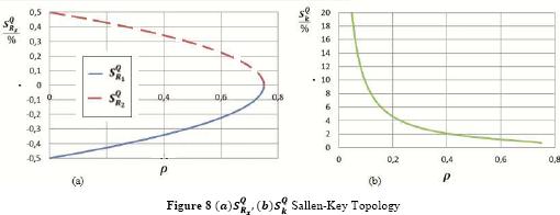
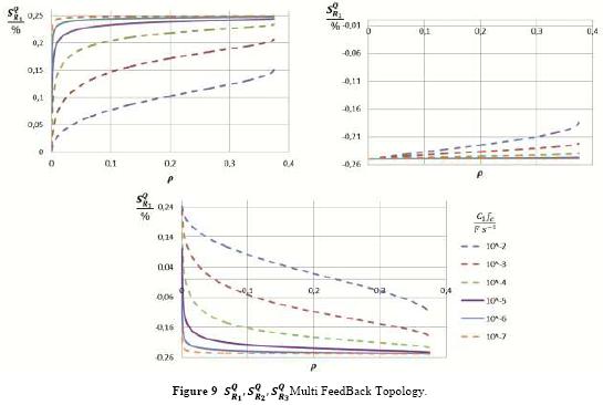
For such reason, frequency response of the Bessel type was selected, whose transfer function for a second order Table 1, in Figure 8 are presented the behaviors for the Sallen-Key topology, whose sensitivities are independent of fc, and in Figure 9 the behaviors shown for the MFB
In accordance with the procedure described in section 2.4, sensitivities shown in filter is given by (2) and whose denominator is a second degree Bessel polynomial [20]. By matching this with the transfer functions of the topologies, statements contained in Table 2 are generated.
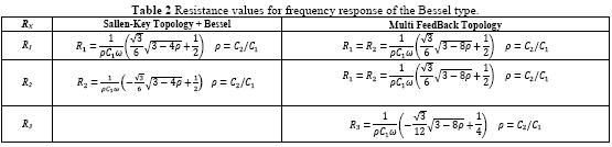

By replacing equations of
Table 2 in the statements of topology, taking into account different orders of magnitude of the product Cifc. (fc is the cut-off frequency of the filter).
3.2. Operating Tests
Figure 10 shows the behavior of the signals when pushing the button P1 (associated to TZ1), imposing a high level for PWM1A and a low level for PWM1B. These levels are predefined in the TZCTL configuration register associated to each PWMxx channel. On the other hand, resulting signal of the voltage booster was captured in channel 3 of the oscilloscope, which is responsible for increasing the amplitude up to 15 V.
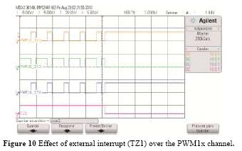
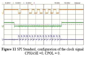
Figure 11 shows the transmission of the word "hexadecimal 7555", along with a configuration mode of the clock signal (0,0), that is to say, the bit transmission is given by each rising edge without delay. MISO signal is captured in channel 1 of the oscilloscope for which the logic level at an idle state is high and a transmission rate of 300 kbps. Channels 2 and 3 respectively record SS and SCLK signals.
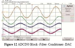
On the third test the ADC module was used, in which a sinusoidal input signal to the filter entrance was introduced with a frequency corresponding to the cutoff frequency (600 Hz), with amplitude of 15 V (Figure 12, Ch1). Channel 2 has the output signal of the filter with amplitude 10 V. Subsequently, the test signal is attenuated 10% and elevated to a DC level of 1.5 V, effectively obtaining a signal amplitude of 1V and 1.5V above the reference of channel 3 (Ch3). Finally, the test signal is digitized at a sampling rate of 735.3 ksps and transmitted to the DAC module for its conversion to analog (channel 4, Ch4).
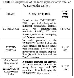
3.3 Comparison with similar boards commercially available
Although on the market there is a variety of development kits, evaluation boards and prototypes training, these are designed for general purpose applications, thus limiting the scope that can be achieved, since they include peripherals that are not specific for power electronics applications, taking up space on the PBC which can be used for conditioning or addition of related modules.
Table 3 shows those commercially available boards, similar to the ones developed in this project. Even though these are specific boards, do not include conditioning of their peripherals such as: different voltage levels for the PWM signals and specific purpose inputs/outputs, antialiasing filters and signal conditioning for the ADC module. Another factor to consider is the cost per unit, due to the 50% decrease compared with the cheapest board registered on Table 3.
4. Conclusions
A development board for power electronics applications based on the Texas Instrument TMS320F28335 DSP, which meets the proper characteristics to developments of prototype and research was designed and implemented. It has the necessary circuitry for setting and conditioning of different modules associated to the DSP (PWM, DAC, ADC, SPI, I2C, CAN, SCI, eQEP, eCAP, GPIO) assembled on a PCB, which was designed based on recommendations made by international organizations and scientific articles published in the IEEE to counter the adverse effects of electromagnetic interference.
Acknowledgments
This paper is the result of the research project "Design and implementation of a development board with digital signal processor and specific purpose in power electronics applications" ("Diseno e implementación de una tarjeta de desarrollo con procesador digital de senales, de propósito específico en aplicaciones de electrónica de potencia") partially funded by the Research and Scientific Development Center of the Universidad Distrital.
References
[1] Varun, R. Prakash y I. Krishnan Bhat, «Energy, economics and environmental impacts of renewable energy systems,» Renewable and sustainable energy reviews, vol. 13, n° 9, pp. 2716-2721, 2009. [ Links ]
[2] P. K. Steimer, «Enabled by high power electronics Energy efficency, renewables and smart grids,» de Power Electronics Conference (1PEC), 2010 International, Sapporo, 2010. [ Links ]
[3] Y. Huang, J. Li y R. Gong, «A novel SVPWM control Stand-alone Three-phase PV power system based on TMS320F28335,» de Consumer Electronics, Communications and Networks (CECNet), 2012 2nd 1nternational Conference on, Yichang, 2012. [ Links ]
[4] J. Salazar, «Procesadores digitales de senal (DSP),» Mundo electronico, n° 314, pp. 46-57, 200. [ Links ]
[5] Texas Instruments, «Data Manual: TMS320F28335, TMS320F28334, TMS320F28232, Digital signal controllers (DSCs),» Texas Instruments, 2007. [ Links ]
[6] P. Embree, C algorithms for real-time DSP, Prentice Hall, 1995. [ Links ]
[7] A. S. Sedra y K. C. Smith, Circuitos Microelectrónicos, Oxford: Oxford University Press, 1999. [ Links ]
[8] H. G. Dimopoulos, Analog Electronic Filters: theory, design amd synthesis, Springer, 2012. [ Links ]
[9] S. Muralikrishna y S. Sathyamurthy, «An overview of digital circuit design and PCB design guidelines - An EMC perspective,» de Electromagnetic Interference & Compatibility, 2008. INCEMIC 2008. 10th International Conference on, Bangalore, 2008. [ Links ]
[10] N. L. Eastman, «Considerations for mixed analog/digital PCB design,» de WESCON/96, Anaheim, 1996. [ Links ]
[11] J. Jing y K. Lingwen, «Study of signal integrity for PCB level,» de Electronic Packaging Technology & High Density Packaging (ICEPT-HDP), 2010 11th International Conference on, Xi'an, 2010. [ Links ]
[12] J. López Sánchez, F. A. Rojas S., C. L. Trujillo y J. Guacaneme Moreno, «Recomendaciones para el diseno de circuitos impresos de potencia,» Revista Cientifica y Tecnologica de la Facultad de Ingenieria Universidad Distrital Francisco José de Caldas, vol. 9, n° 2, pp. 44-47, 2003. [ Links ]
[13] See, «Impact of PCB Layout Design on Final Product's EMI Compliance,» de 17th International Zurich Symposium on Electromagnetic Compatibility, Zurich, 2006. [ Links ]
[14] P. Chand, B. N. Gangopadhyay y M. Kumar, «PCB layout design for EMI/EMC compliance,» de Electro Magnetic Interference and Compatibility (INCEMIC), 2006 Proceedings of the 9th 1nternational Conference on, Bangalore, 2006. [ Links ]
[15] W. Saraga, «Sensitivity of 2nd-order Sallen Key type active RC fiteis,» Electronics Letters, vol. 3, n° 10, pp. 442-444, 1967. [ Links ]
[16] W.-. K. Chen, Passive, Active and digital filters, CRC Press, 2005. [ Links ]
[17] F. Miyara, Filttos Activos. E-book, Rosario: Universidad Nacional de Rosario, 2004. [ Links ]
[18] P. Horowitz y W. Hill, The art of electronics- 2nd Edition, Cambrige University Press, 1989. [ Links ]
[19] M. Thompson, Intuitive Analog circuit design, 2nd Edition, Nownes, 2013. [ Links ]
[20] J. L. Dominguez Barragan, «Acondicionamiento de filters,» Universidad de las Americas Puebla, Puebla, 2003. [ Links ]
