


 English (pdf)
 Article in xml format
 Article references
 Send this article by e-mail
 Cited by SciELO
  Cited by Google
  Similars in
SciELO
Similars in
SciELO  Similars in Google
 Permalink
1. Introduction
Currently, most electronic equipment such as power sources, battery chargers, appliances, communication systems, medical equipment, among others, need a constant DC voltage bus from the AC line. For this they include in the input stage the simplest and most conventional AC-DC converter (SC), which comprises a diode bridge and an electrolytic capacitor with a high capacitance value [1]. The SC is widely used because of its very low cost; however, the waveform that the converter absorbs from the AC line is not sinusoidal and has a high crest factor, due to the small conduction angle used by the electrolytic capacitor to charge [2]. For this reason, the waveform of the line current has a high total harmonic distortion that produces the following disadvantages: first, reduction of the power factor, which implies a decrease in the AC line available power [3]; second, harmonics injection to the line voltage that interfere with other electronic equipment connected to the same line [4]; finally, line voltage instability [5].
Consequently, the SC cannot meet the IEC-61000-3-2 and IEEE Std 519 European and/or American standard respectively. These standards impose the limits on AC current harmonics, as well as in total harmonic distortion of the electronic equipment that is fed by the AC line [6]. In order to meet these standards, different studies in the area of power electronics have focused on improving the power factor of electronic equipment that are connected to the line.
For this purpose, AC-DC converters with power factor correction (CPFC) are the best alternative [7] [8]. Several authors have analyzed the operation of the CPFC topologies, from the most classic such as: boost [9] [10], buck-boost [11], flyback [12] [13] and half bridge boost [14] [15], up to the most recent: no diode bridge [2] [16] [17], interleaved [18] and flyback with dual-purpose inverter [19]. Within these, the AC-DC converters with power factor correction in half bridge boost topology (CPFC-HBB) has the simplest conversion circuit and with fewer switches[20], so the main advantage of the CPFC-HBB is that it presents high efficiency, since at any time there is only a voltage drop, which is produced by the working semiconductor [21]. Another advantage of the CPFC-HBB is to allow its power flow to be bidirectional; this explains why the CPFCHBB is widely used in power factor correction applications [22].
On the other hand, other authors have studied and implemented control methods for the CPFC-HBB such as: conventional analog [7], by replacing a boost diode and inductor with a switch and transformer, respectively [23], current-by hysteresis [14] [24], non-linear Lyapunov technique [25] [26] and non-linear carrier control [27] [28], or current sensor-less control [29].
The emergence of low-cost microprocessors, digital signal processors (DSP) and programmable gate array (FPGA) has made it possible for new control strategies to emerge, which have advantages such as programmability and lower sensitivity to parameters variation. Some of these control strategies that predict the CPFC duty cycle from the inductance, reference current, input voltage and output voltage reference, have been introduced in previous works [30] [31], nevertheless, these control strategies were implemented in CPFC in boost topology .
In this work, we propose a strategy for predicting the duty cycle for a CPFC-HBB, in order to obtain a high power factor. The aim of this work is to design a control strategy for CPFC-HBB, by means of predicting the duty cycle starting from the average model. This work is divided as follows: in Section 2, a rigorous and detailed analysis of the proposed control strategy is presented using the average circuit model; in section 3, the simulation results of the proposed control that was implemented in MATLAB R Simulink; in section 4, the conclusions and future work.
2. Predictive Control Strategy for a CPFC-HBB
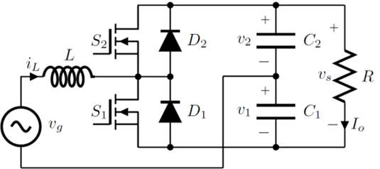
The CPFC-HBB circuit used with the predictive control strategy is shown in Fig. 1. The CPFC-HBB consists of two switches, in this case MOSFET's (S1, S2) each with their respective intrinsic diode, an inductance on the AC side (L), two capacitors on the DC side (C 1, C 2) and a load resistance (R).
The analysis of the proposed control strategy is derived from assuming that all CPFC-HBB circuit components are ideal. To begin with, the inductance voltage equation that is given by:
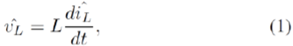
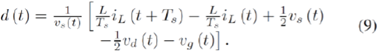
Here i ^ L and v ^ L are the instantaneous current and voltage of the inductance respectively. By solving for i ^ L and integrating from t to t + Ts:
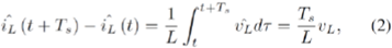
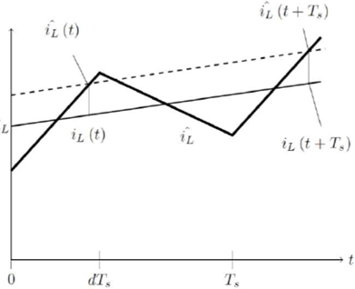
Here i ^ L (t) is the initial current in the inductance and i ^ L(t + T s ) is the desired current at the end of the period to achieve a unit power factor in the CPFC-HBB. In [20] it was determined that the left side of equation 2 is the net change in the inductance current over a switching period, also noting that said change is exactly equal to the switching period for the average slope.
On the other hand, Fig. 2 shows the average circuit model (ACM), in which the switches are replaced by controlled sources [20]. S 1 is replaced by a voltage source whose value is equal (1 - d) vs, where d is the duty cycle of S1 and v s is the sum of the average voltages of capacitors v¡ and v2, likewise, S 2 is replaced by a current source with value equal to (1 - d) iL, where iL is the average current of the inductance.
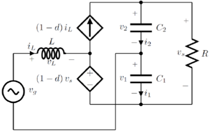
The ACM is used to obtain expressions that define the state equations averaged over one switching period, to determine the steady-state values CPFC-HBB easily and finally, to simulate efficiently the CPFC-HBB, this means that time and memory storage decreases compared to the simulation using the switches. However, the switch model is useful and necessary to determine currents and peak voltages experienced by the CPFC-HBB.
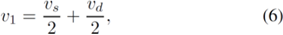
When applying Kirchhoff's law of voltages around the ACM mesh, composed of vg, L, (1 - d) v s and C1, we obtain the average voltage of inductance VL, which is defined by:

The averaged state variables of the CPFC-HBB are iL, v 1 and v 2 . However, the voltage in the load resistance is vs, for this reason the state variables v 1 and v 2 are changed to the new state variables v s and v d , which respectively represent the capacitors voltage sum and voltage difference. The state variable iL stays the same, then v s and v d are defined by:
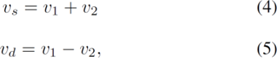
Solving v¡ from equations 4 and 5:
By substituting equation 6 in 3:
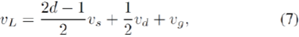
Replacing equation 7 in 2, the duty cycle d is given by:
When observing Fig. 3, it is established that the net change in the inductance current over a switching period can be expressed in terms of the average input current ÍL, hence, equation 8 becomes:
The value of the duty cycle can be known, as long as all the variables to the right of equation 9 are known. However, the inductor current at the end of the switching period iL (t + Ts) is unknown. In order to obtain a unit power factor in the CPFC-HBB, the value of this current must be proportional to the input voltage v g value evaluated in t + T s . Although this voltage is also unknown, it can be replaced by the input voltage vg evaluated in t, hence, if the switching frequency is much higher than the input voltage frequency, thus, we can say that v g (t) is a good approximation of vg (t + Ts), so that equation 9 is changed to:
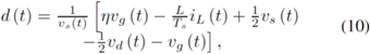
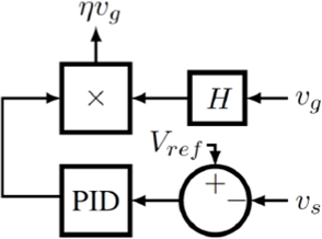
Here ηv g is the reference current and η is the peak value of the reference current that governs the output voltage vs, η is also the product, as shown in Fig. 4, between the output of the PID regulator block that is in the loop that controls v s and the gain of block H, which serves to take a sample of the input voltage v g to the multiplier.
We should also mention that the output voltage is controlled to follow the reference voltage V ref , therefore, the output voltage vs becomes a constant value equal to V ref and the division by v d (t) which is performed in equation 10 is no longer necessary, thus, duty cycle d can be expressed as:
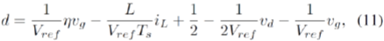
The duty cycle d in equation 11 processes the current average values of the reference current ηv g , the inductance iL, the input voltage v g current and the voltage difference v d, together with the constant terms mentioned above; likewise, it is shown in equation 11 that only four multiplications and five additions are needed to implement the computation of d.
The inductance current is controlled by d, so that it follows the reference current, with the purpose that the power factor is unitary. However, in t + T s the inductance current iL is not exactly the same, but very close to the reference current ηv g .
The block diagram of the pulse width prediction control (PWPC) proposed for the CPFC-HBB is shown in Fig. 5. This diagram shows how block d implements the calculation of equation 11, also, it shows that the duty cycle calculated d by that block passes through a ZOH zero-order hold before entering the pulse width modulator block SPWM, which holds d within a switching period T s .
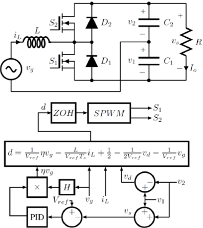
With the proposed PWPC, the current inductance iL of the CPFC-HBB follows the reference current and the output voltage vs of the CPFC-HBB follows the reference voltage. On the other hand, [9] confirmed the existence of the voltage imbalance in the capacitors; they also researched the causes that produced it and provided a control scheme to eliminate it, this scheme consists in adding the difference between v 1 and v 2 to the reference current multiplied by a gain. The PWPC proposed in this work, eliminates the capacitor voltage imbalance, since as can be seen in Fig. 5, it has this control scheme in its block diagram. The work of [9] suggests that the value of the block gain processing the difference between v' and v2 must be less than or equal to 0.1 ωC, being ω the angular frequency of vg, and C the capacitance value of any of the capacitors, so that the voltage imbalance is zero.
3. Results
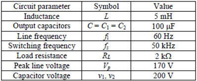
A CPFC-HBB with the proposed PWPC strategy was simulated using MATLAB R Simulink, with the circuit parameters that are shown in Table 1, likewise, it was considered that the input voltage is sinusoidal.
The experimental results show that a high power factor is obtained under stationary and transient conditions, these results are shown in subsections 3.1 and 3.2.
3.1 Test results in steady state
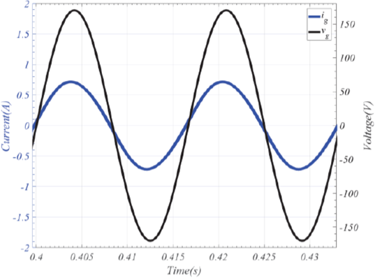
Voltage and the input current (v g and i g ) waveforms of the CPFC-HBB with maximum load current I o = 200 mA, are shown in Fig. 6.
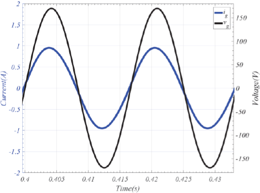
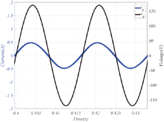
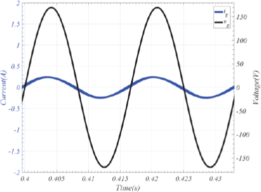
The power factor (PF) with this load condition is 0.9954 and the total harmonic distortion (THD) is 2%. The waveforms v g and i g for Io = 100 mA, are shown in Fig. 8, the PF with this load condition is 0.9913 and the THD is 3.1 %. The waveforms v g and i g for Io = 50 mA, are shown in Fig. 9, the PF with this load condition is 0.9796 and the THD is 5.6 %. Also, when looking at Figs. 6-9, it can be stated that as the load increases the PF increases, and at the same time, the THD decreases.
Test results show that the proposed control method for CPFC-HBB, can achieve a near unit power factor and low total harmonic distortion, in steady state condition and with different load current values. In this way, the proper functioning of the PWPC proposed in steady state is shown. Increased in step from 150 mA to 200 mA is shown in Fig. 10. Note that the duration of the transient is 40 ms and the voltage drop of v1 and v2 is around 10 V.
3.2 Test results in transient state
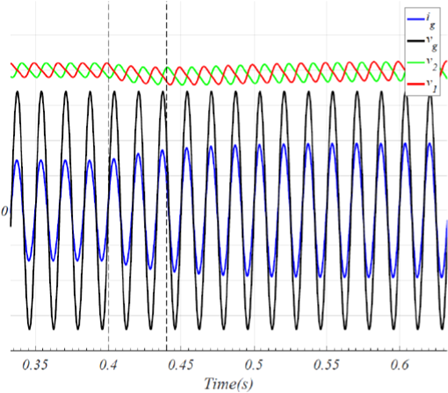
Likewise, when I o is decreased in step from 200 mA to 150 mA is shown in Fig. 11. Note that the duration of the transient is 48.5 ms and the voltage overshoot of v1 and v2 is around 10 V. On the other hand, the transient response when vg is increased in step from 120V to 140 V, is shown in Fig. 12. We can see that the duration of the transient is 50 ms and the voltage overshoot of v1 and v2 is around 10 V.
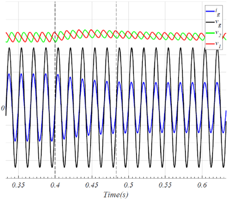
Figure 11 i g , v1 and v2 waveforms in load transient state; I o changed from 200 mA to 150 mA, v g = 50 V/div, v 1 and v 2 = 50 V/div, i g = 1 A/div.
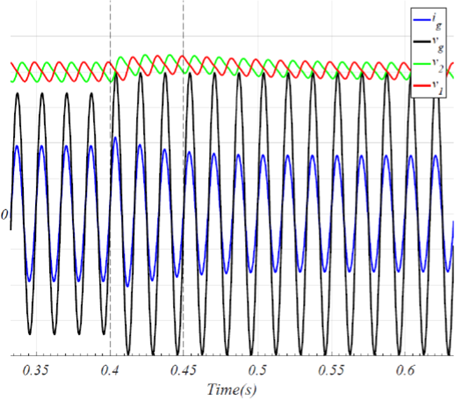
Figure 12 ig, v1 and v2 waveforms for step input voltage change; v g changed from 120 V to 140 V, v g = 50 V/div, v 1 and v 2 = 50 V/div, i g = 1 A/div.
Similarly, the transient response when vg is reduced in step from 140 V to 120 V is shown in Fig. 13. Note that the transient period is 50 ms and the voltage drop of v1 and v2 is around 10 V. In addition, in Figs. 10-13, we can see that within the transient periods, the input current remains sinusoidal. We can also see that v 1 and v 2, are absolutely equal in the steady state and transient conditions, this confirms what was said in section 2, that the proposed control includes the scheme that was presented in [9], to eliminate the problem of voltage imbalance in capacitors.
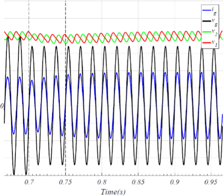
Figure 13 i g , v 1 and v2 waveforms for step input voltage change; v g changed from 140 V to 120 V, v g = 50 V/div, v 1 and v 2 = 50 V/div, i g = 1 A/div.
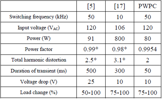
Table 1 shows the performance comparison of the CPFCHBB parameters obtained in simulation, with the proposed control method and other works reported previously. Among these studies, is the one presented in [5], where the analysis is shown in detail CPFC-HBB, and the implementation of internal current loop with current averaging technique using a PID controller; the work presented in [17] is also included, where a simple analog control was proposed and implemented for the CPFC-HBB with the non-linear carrier control method.
Observing Table 2, the following can be stated: first, the power factor of the CPFC-HBB with the proposed PWPC is higher than power factors obtained in [5] [17]; second, the total harmonic distortion of the CPFC-HBB with the proposed PWPC is lower compared to [5] [17]; third; the transient response of CPFC-HBB with PWPC proposed is much faster than that presented in [5] [17]; finally, the voltage drop of the CPFC-HBB capacitors with the proposed PWPC is the same as in [17] and lower than in [5].
4. Conclusions
In this paper we presented a control technique for the prediction of the pulse width applied to an AC-DC converter with power factor correction, in half bridge boost topology.
The results show a power factor of 0.9954, transient response times to load change from 75% to 100% and THD of 2%, which are comparable with values reported in literature using techniques based on classic control laws. This implies that the proposed technique can achieve satisfactory results without revising performance parameters, or perform stability analysis.
It is also noteworthy that the algorithm proposed for the duty cycle prediction was obtained from the variables of state and average input, since it was based on the ACM. This implies an advantage over the techniques reported in literature that use instantaneous values of these variables, making measurement more difficult.
In future work, the converter will be implemented in hardware with the proposed control technique, verifying the results experimentally and comparing the resulting power factor with other existing techniques. In addition, the algorithm will be implemented to other topologies of AC-DC converters with power factor correction

