SciELO - Scientific Electronic Library Online

 
vol.15 número28Tendencia de la calidad del aire y propuesta de una aplicación web para la red de monitoreo atmosférico en Tabasco, México.Representación del Modelo Semántico en el Derecho Informático índice de autoresíndice de materiabúsqueda de artículos
Home Pagelista alfabética de revistas  

Servicios Personalizados

Revista

Articulo

Indicadores

Links relacionados

  • En proceso de indezaciónCitado por Google
  • No hay articulos similaresSimilares en SciELO
  • En proceso de indezaciónSimilares en Google

Compartir


Tecciencia

versión impresa ISSN 1909-3667

Tecciencia vol.15 no.28 Bogotá ene./jun. 2020  Epub 17-Dic-2020

https://doi.org/10.18180/tecciencia.28.3 

Articles

Stability Performance of a Quantum Square-shaped Extended Source P-N-P-N TFET with Silicon Carbide Substrate by Means of a Physics-Based Analytical Model

Desempeño de Estabilidad de una Fuente Cuántica Cuadrada Extendida P-N-P-N TFET con Sustrato de Carburo de Silicio Mediante un Modelo Analítico Físico

Masoud Sabaghi1  *** 

1 Photonics and Quantum Technologies Research School, Nuclear Science and Technology Research Institute (NSTRI), Atomic Energy Organization of Iran (AEOI), Tehran, Iran, 141551339.


ABSTRACT

ABSTRACT. In this paper, an analytical stability model for quantum square-shaped extended source P-N-P-N tunneling field-effect transistor (P-N-P-N TFET) with silicon carbide substrate is developed that includes the effects of gate-source capacitance, gate-drain capacitance, effective gate resistance, time constant and transconductance. A nonquasistatic RF small-signal model has been used and stability that was extracted from analytical equations of its Y-parameters. The obtained analytical expression for stability is compared with device simulation results and excellent agreement is found up to 100 GHz. The stability performance of a quantum square-shaped extended source P-N-P-N TFET with silicon carbide substrate is also studied analytically considering pocket width and doping variation. The results strongly confirm that the proposed model is accurate and suitable for the quantum square-shaped extended source P-N-P-N TFET in the high-frequency regime

Keywords: Analytical modeling; Nonquasistatic (NQS); Quantum extended source, stability; silicon carbide; P-N-P-N Tunneling field-effect transistor (P-N-P-N TFET)

RESUMEN

RESUMEN. En este documento, se desarrolla un modelo de estabilidad analítica para el transistor de efecto de campo de túnel PNPN de fuente extendida cuántica de forma cuadrada (PNPN TFET) con sustrato de carburo de silicio que incluye los efectos de la capacitancia de fuente de compuerta, capacitancia de drenaje de compuerta, resistencia efectiva de compuerta, constante de tiempo y transconductancia. Se ha utilizado un modelo de señal pequeña RF no cuantitativo y una estabilidad que se extrajo de las ecuaciones analíticas de sus parámetros Y. La expresión analítica obtenida para la estabilidad se compara con los resultados de la simulación del dispositivo y se encuentra que los resultados coinciden bien hasta 100 GHz. El rendimiento de estabilidad de un TFET P-N-P-N de fuente extendida cuántica con sustrato de carburo de silicio también se estudia analíticamente considerando el Pocket-Width y la variación de dopaje. Los resultados confirman que el modelo propuesto es preciso y adecuado para la fuente extendida cuántica de forma cuadrada P-N-P-N TFET en el régimen de alta frecuencia

Palabras clave: Modelos analíticos; No cuasi-estático (NQS); Fuente cuántica extendidad, Estabilidad; Carburo de silicio; P-N-P-N Transistor de efecto de campo de túnel (TFETP-N-P-N)

INTRODUCTION

Tunneling field-effect transistors (TFETs) based on band-to-band tunneling (BTBT) mechanism are considered to be a promising solution to the downscaling and power crisis of the complementary metal oxide semiconductor (CMOS) in low standby power (LSTP) devices. In particular, TFETs can achieve sub-60 mV/decade subthreshold slope (SS) at room temperature, enabling ultralow power dissipation and suppressed short channel effects (SCE) [1,2,3]. A lot of research has been done in the area of TFETs in terms of the design, modeling, fabrication, and characterization [4]-[28]. The stability is one of the important parameters in the selection of transistor to design the radio-frequency (RF) amplifier and integrated circuit. Generally, there are two possible types for devices stability. One is the unconditionally stable device that is preferred for the RF design because its stability is port impedance-independent. The other is potentially stable device that causes significant performance degradation and the noise level increase, due to need of additional stabilization network. Marjani et al. presented the RF small-signal model for square-shaped extended source tunneling field-effect transistor in the context of careful consideration of gate-source capacitance, gate-drain capacitance, effective gate resistance, time constant and transconductance using a combination of nonquasistatic RF small-signal modeling, device simulations, and SPICE verification [20].

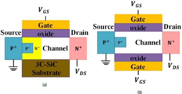
FIG. 1 Cross-section views of the (a) quantum square-shaped extended source P-N-P-N TFET with silicon carbide substrate, (b) conventional square-shaped extended source TFET structures. 

In this paper, an analytical stability model for quantum square-shaped extended source P-N-P-N tunneling field-effect transistor (P-N-P-N TFET) with silicon carbide substrate is developed that includes the effects of gate-source capacitance, gate-drain capacitance, channel resistance, time constant and transconductance. The stability was extracted from analytical equations of Y-parameters that were evaluated by two-dimensional device simulator simulation using stimulating multiple models including nonlocal band-to-band tunneling model, auger recombination, trap assisted tunneling model, band-gap narrowing, Shockley-Read-Hall recombination model, Hurkx recombination model, concentration dependent mobility model and field dependent mobility model. The paper is organized as follows: Section 2 describes the device structures and model formulation of stability for quantum square-shaped extended source P-N-P-N TFET. Section 3 presents the model validation, results and discussion. In Section 4, we conclude.

2 | DEVICE STRUCTURE AND MODEL FORMULATION OF STABILITY FOR QUANTUM SQUARE-SHAPED EXTENDED SOURCE P-N-P-N TFET

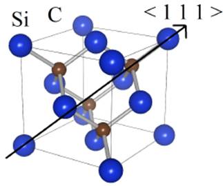
Fig. 1 (a) and (b) show cross-sectional views of the quantum square-shaped extended source P-N-P-N TFET with silicon carbide substrate and conventional square-shaped extended source TFET devices for simulations in Silvaco ATLAS software [29]. The heavily doped pocket and square-shaped extended source regions can be achieved by a tilt angled implant before the gate stack formation and high-energy and low-current boron implantation after the pocket formation [6][20]. The 3C-SiC is one of silicon carbide polytypes that have been concerned as the today's semiconductor materials. It has the high electron mobility and saturation velocity because of the reduced scattering [30] that its lattice structures is shown in Fig. 2.

FIG. 2 The crystal structure of cubic silicon carbide polytype (3C-SiC). 

The simulated devices are the channel doping concentrations 1015 cm -3, source doping concentrations 1020 cm -3, drain doping concentrations 1020 cm -3, pocket doping concentrations 1019 cm -3, body thickness of 15nm, 2nm gate oxide thickness and 30nm of gate length.

The Y-parameters of the nonquasistatic RF small-signal model for square-shaped extended source tunneling field-effect transistor in the context of careful consideration of gate-source capacitance (C gs), gate-drain capacitance (C gd ), effective gate resistance (R g ), time constant (t) and transconductance (g m) can be expressed as [20]:

Y11= ω2Rg  (Cgs+ Cgd)2+jω(Cgs + Cgd)1+ ω2 Rg2 (Cgs + Cgd)2 , (1)

Y12= - ω2 Rg Cgd Cgs+ Cgd -jωCgd1+ ω2 Rg2 (Cgs+ Cgd)2 , (2)

Y21= -jωCgd- ω2 Rg Cgd (Cgs+ Cgd)1+ ω2 Rg2 (Cgs+ Cgd)2+ gm-jωgm T+Rg Cgs+ Cgd- ω2RggmT(Cgs+ Cgd)[1+ω2Rg2 Cgs+ Cgd)2 (1+ ω2T2), (3)

And

Y22= -jωCgd-ω2RgCgd(Cgs+Cgd)1+ ω2Rg2 (Cgs+Cgd)2+gm-jωgm T+Rg Cgs+ Cgd-ω2RggmT(Cgs+Cgd)[1+ω2 Rg2 (Cgs+ Cgd )2](1+ω2T2) (4)

where {Y mn } with m = 1,2 and n = 1,2 are complex parameters and j = √-1 is the imaginary unit. By using real and imaginary parts of Eqs. 1-4 and considering some assumptions, The analytical values of device small signal parameters can be obtained as [20]:

gm=ReY21|ω2=0 ,  (5)

gds=Re[Y22]|ω2=0 ,  (6)

Rg=1(lm[Y11])2ReY11 ,  (7)

Cgs= -1ω lmY11+lm[Y12] ,  (8)

Cgd=- 1ω lmY12 ,  (9)

T= -1gmlmY12 ω + Cgd+ gm+ Rg Cgs+ Cgd ,  (10)

and

Cds= 1ω lmY22 - Cgd- RggmCgd.  (11)

The stability of TFET can be expressed at different frequencies of operation in terms of Y-parameters as follows [31]:

k 2Re[Y11]ReY22-Re[Y12Y21][Y12Y21 ]  (12)

In order to simplify further, by substituting the Y-parameters into (12), the analytical equations for stability are obtained as a function of the small-signal parameters as below:

k= ω2(Cgd2+2Cgs+CgdCgsgds+Cgdgds+gmRg+CgdgmTgm2+(Cgd+gmT)2ω2 (Cgdω+Cgd(Cgs+Cgd)2Rg2ω3)+ ω4Cgd(Cgs+Cgd)2Rg2(Cgd+2CgdgmRg+gm2CgsRg+T)gm2+(Cgd+gmT)2ω2(Cgdω+Cgd(Cgs+Cgd)2Rg2ω3)   (13)

3 | MODEL VALIDATION, RESULTS AND DISCUSSION

To verify the validity of the proposed model, stability of the quantum square-shaped extended source P-N-P-N TFET with silicon carbide substrate and conventional square-shaped extended source TFET devices are simulated using the Silvaco ATLAS device simulator [29]. Fig. 3 compares the stability that were obtained from the analytical model and the simulated values as a function of the frequency for the quantum square-shaped extended source P-N-P-N TFET with silicon carbide substrate (Structure A) and conventional square-shaped extended source TFET (Structure B) with 30nm gate length in the on-state (V g = 1.5V and V d = 1V). As seen, an excellent agreement for the stability of analytical model and device simulation is achieved up to the 100GH z regime. In addition, the quantum square-shaped extended source P-N-P-N TFET with silicon carbide substrate has higher shows a better stability compared to conventional square-shaped extended source TFET because of its higher transconductance and gate-drain capacitance. Without any optimization, the root mean square (RMS) error of the model was calculated to be within 1.25% up to 100GH z. These verification results strongly support that the model is accurate and valid for quantum square-shaped extended source P-N-P-N TFET with silicon carbide substrate and conventional square-shaped extended source TFET up to the extremely high frequency range.

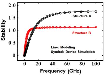
FIG. 3 Comparison of modeling and device simulation values of stability for quantum square-shaped extended source P-N-P-N TFET with silicon carbide substrate (Structure A) and conventional square-shaped extended source TFET (Structure B) structures. 

In addition, we analyze analytically the dependence of the stability on pocket parameters including width and doping variation. Fig. 4 shows the impact of varying width of pocket (W) with constant doping concentration of 1 x 10-19cm-3 on the stability of a quantum square-shaped extended source P-N-P-N TFET biased at V d = 1V. Five different values of pocket width 1,2,3,4 and 5nm, are used for this purpose. On one hand, on-current and transconductance of device increases as pocket width increases. This is mainly because the well region containing the local minimum of the conduction energy band edge becomes wider, which increases the probability of the tunneling of electrons from source to drain, and thus on-current increases. But on the other hand, an increasing pocket width results in increasing gate-drain capacitance. Especially for very wide pocket width, pocket begins to be partially depleted and declines the on-current and transconductance. Since pocket width of 2 produces the best performance of the stability, it is used for the rest of this paper. Also, the critical frequency values of above-mentioned devices with 1,2,3,4 and 5nm pocket width are about 13.3,13.5,11.7,8.3 and 6.7GH z, respectively. This indicates that the quantum square-shaped extended source P-N-P-N TFET does not require the additional stability circuits for RF circuits above these frequencies. This model fits well with RMS error within 1.13% up to 100GH z.

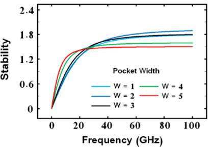
FIG. 4 Variation of stability of quantum square-shaped extended source P-N-P-N TFET versus frequency for various values of pocket width. 

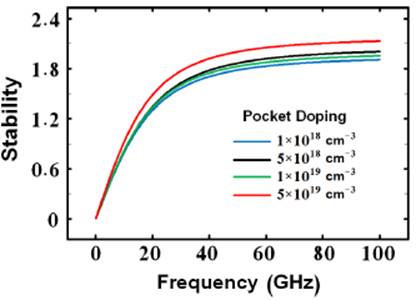
Fig. 5 shows the stability for four different values of pocket doping concentration (N p) as 1 x 10¹⁸, 5 x 10¹⁸, 1 x 10¹⁹, and 5 x 1019cm-3 with constant width of 2nm. As seen, the use of relatively high pocket doping concentration results in the enhancement of stability. This is mainly because of the high on-current and transconductance induced by the narrower tunneling barrier width at the source-channel interface. It is also observed that the pocket doping concentration plays an important role in determining the critical frequency. The value of critical frequency reaches 13 GHz for lower pocket doping concentration (N p = 1 x 1018 cm -3) as compared to higher pocket doping concentration (N p = 5 x 1019 cm -3) with critical frequency greater than 10GH z. The RMS error between modeled and simulated values for four different values of pocket doping concentration is only 1.65%. The results of model verification confirm that the model is highly reliable and available for the quantum square-shaped extended source P-N-P-N TFET with silicon carbide substrate.

FIG. 5 Variation of stability of quantum square-shaped extended source P-N-P-N TFET versus frequency for various values of pocket doping concentration. 

4 | CONCLUSION

In this paper, we develop an analytical stability model for quantum square-shaped extended source P-N-P-N TFET with silicon carbide substrate by considering the effects of gate-source capacitance, gate-drain capacitance, effective gate resistance, time constant and transconductance. The analytical expression of stability is obtained from Y-parameters equations of a nonquasistatic RF small-signal model. The stability performance of a quantum square-shaped extended source P-N-P-N TFET with silicon carbide substrate is compared with the conventional square-shaped extended source TFET and excellent agreement is found up to 100 GHz. In addition, the width and doping dependence of pocket on performance of the quantum square-shaped extended source P-N-P-N TFET with silicon carbide substrate has been studied. The results indicate that the proposed model is accurate and suitable for the quantum square-shaped extended source P-N-P-N TFET with silicon carbide substrate in the high-frequency regime up to 100 GHz.

References

[1] A. Ionescu and H. Riel, "Tunnel field-effect transistors as energy-efficient electronic switches," Nature, vol. 479, no. 7373, pp. 329-337„ 2011. DOI: 10.1038/nature10679. [ Links ]

[2] B. Rajamohanan, D. Mohata, A. Ali, and S. Datta, "Analysis of trap-assisted tunneling in vertical si homo-junction and sige hetero-junction tunnel-fets," Solid State Electron, vol. 83, pp. 50-55„ 2013. DOI: 10.1016/j.sse.2013.01.026. [ Links ]

[3] T. A. Ameen, H. Ilatikhameneh, P. Fay, A. Seabaugh, R. Rahman, and G. Klimeck, "Alloy engineered nitride tunneling field-effect transistor: A solution for the challenge of heterojunction tfets," IEEE Transactions on Electron Devices, vol. 66, no. 1, pp. 736-742, 2018. DOI: 10.1109/TED.2018.2877753. [ Links ]

[4] K. Boucartand A. Ionescu, "Double-gate tunnel fet with high-k gate dielectric," IEEE Trans. Electron Devices, vol. 54, no. 7, pp. 1725-1733„ 2007. DOI: doi.org/10.1109/TED.2007.899389. [ Links ]

[5] B. Dorostkar and S. Marjani, "Dc analysis of p-n-p-n tunneling field-effect transistor based on in0.35ga0.65as," HOLOS, vol. 34, no. 1, pp. 288-296„ 2018. DOI: 10.15628/holos.2018.6173. [ Links ]

[6] S. Marjani , S. Khosroabadi, and S. Hosseini, "Enhanced characteristics of square-shaped extended source tfet via silicon carbide polytype (3c-sic) and a dopant pocket layer," Orient. J. Chem, vol. 33, no. 3, pp. 1083-1089„ 2017. DOI: 10.13005/ojc/330303. [ Links ]

[7] A. Vallett, S. Minassian, P. Kaszuba, S. Datta , J. Redwing, and T. Mayer, "Fabrication and characterization of axially doped silicon nanowire tunnel field-effect transistors," Nano let, vol. 10, no. 10, pp. 4813-4818„ 2010. DOI: doi.org/10.1021/nl102239q. [ Links ]

[8] G. Dewey, B. Chu-Kung, J. Boardman, J. Fastenau, J. Kavalieros, W. Liu, D. Lubyshev, M. Metz, N. Mukherjee, P. Oakey, R. Pillarisetty, M. Radosavljevic, H. Then, and R. Chau, "Fabrication, characterization, and physics of iii-v heterojunction tunneling field effect transistors (h-tfet) for steep subthreshold swing"," in IEEE international electron device meeting (IEDM, (Washington, DC, USA), pp. 5-7„ 2011. DOI: 10.1109/IEDM.2011.6131666. [ Links ]

[9] L. Britnell, R. Gorbachev, R. Jalil, B. Belle, F. Schedin, A. Mishchenko, T. Georgiou, M. Katsnelson, L. Eaves, S. Morozov, N. Peres, J. Leist, A. Geim, K. Novoselov, and L. Ponomarenko, "Field-effect tunneling transistor based on vertical graphene heterostructures," Science, vol. 335, no. 6071, pp. 947-950„ 2012. DOI: 10.1126/science.1218461. [ Links ]

[10] B. Dorostkar, M. Mahoodi, and S. Marjani , "Design and simulation of tunnel field effect transistor based on al0.25ga0.75as," in The 2nd Electrical and Computer, Conference on Innovative Researches Development (ECCIRD), Torbat-e Jam, Iran, pp. 1-3„ 2019. [ Links ]

[11] M. Mahoodi , S. Marjani , and B. Dorostkar , "Radio-frequency modeling of double and single gate tfets with silicon carbide polymer," in The 2nd Electrical and Computer, Conference on Innovative Researches Development (ECCIRD), Torbat-e Jam, Iran, pp. 1-3„ 2019. [ Links ]

[12] S. Richter, C. Sandow, A. Nichau, S. Trellenkamp, M. Schmidt, R. Luptak, K. Bourdelle, Q. Zhao, and S. Mantl, "w-gated silicon and strained silicon nanowire array tunneling fets," IEEE Electron Device Lett, vol. 33, no. 11, pp. 1535-1537„ 2012. DOI: 10.1109/LED.2012.2213573. [ Links ]

[13] A. Mallikand A. Chattopadhyay, "Tunnel field-effect transistors for analog/mixed signal system-on-chip applications," IEEE Trans. Electron Devices, vol. 59, no. 4, pp. 888-894, 2012. DOI: 10.1109/TED.2011. 2181178. [ Links ]

[14] S. Marjani , S. Hosseini , and R. Faez, "A silicon doped hafnium oxide ferroelectric p-n-p-n soi tunneling field-effect transistor with steep subthreshold slope and high switching state current ratio," AIP Advances, vol. 6, no. 9,pp, pp. 095010-1-095010-7„ 2016. DOI: 10.1063/1.4962969. [ Links ]

[15] S. Marjani , S. Hosseini , and R. Faez , "A 3-d analytical modeling of tri-gate tunneling field-effect transistors," J. Comput. Electron, vol. 15, no. 3, pp. 820-830„ 2016. DOI: 10.1007/s10825-016-0843-0. [ Links ]

[16] Y. Yang, P. Guo, G. Han, K. Low, C. Zhan, and Y.-C. Yeo, "Simulation of tunneling field-effect transistors with extended source structures," J. Appl. Phys, vol. 111, pp. 114514-1- 114514-8„ 2012. DOI: 10.1063/1.4729068. [ Links ]

[17] L. Lattanzio, N. Dagtekin, L. Michielis, and A. Ionescu , "On the static and dynamic behavior of the germanium electron-hole bilayer tunnel fet," IEEE Trans. Electron Devices, vol. 59, no. 11, pp. 2932- 2938„ 2012. DOI: 10.1109/TED.2012.2211600. [ Links ]

[18] K.-T. Lam, X. Cao, and J. Guo, "Device performance of heterojunction tunneling field-effect transistors based on transition metal dichalcogenide monolayer," IEEE Electron Device Lett, vol. 34, no. 10, pp. 1331-1333„ 2013. DOI: 10.1109/LED.2013.2277918. [ Links ]

[19] K. Kao, A. Verhulst, W. Vandenberghe, and K. Meyer, "Counterdoped pocket thickness optimization of gate-on-source-only tunnel fets," IEEE Trans. Electron Devices, vol. 60, no. 1, pp. 6-12„ 2013. DOI: 10. 1109/TED.2012.2227115. [ Links ]

[20] S. Marjani and S. Hosseini , "Radio-frequency modeling of square-shaped extended source tunneling field-effect transistors," Superlattices and Microstructures, vol. 76, pp. 297-314„ 2014. DOI: 10.1016/j.spmi.2014.09.040. [ Links ]

[21] G. Beneventi, E. Gnani, A. Gnudi, S. Reggiani, and G. Baccarani, "Dual-metal-gate inas tunnel fet with enhanced turn-on steepness and high on-current," IEEE Trans. Electron Devices, vol. 61, no. 3, pp. 776-784„ 2014. DOI: 10.1109/TED.2014.2298212. [ Links ]

[22] S. Marjani and S. Hosseini , "A novel double gate tunnel field effect transistor with 9 mv/dec average subthreshold slope," in 22st Iranian Conference on Electrical Engineering (ICEE, (Tehran, Iran), pp. 399-402„ 2014. DOI: 10.1109/IranianCEE.2014.6999572. [ Links ]

[23] S. Marjani and S. Hosseini , "Rf modeling of p-n-p-n double-gate tunneling field-effect transistors," in 3rd Conference on Millimeter-Wave and Terahertz Technologies (MMWaTT, (Tehran, Iran), 2014. DOI: 10.1109/MMWaTT.2014.7057188. [ Links ]

[24] I. Kwon, M. Je, K. Lee, and H. Shin, "A simple and analytical parameter-extraction method of a microwave mosfet," IEEE Trans. Microwave Theory Tech, vol. 50, no. 6, pp. 1503-1509„ 2002. DOI: 10.1109/TMTT. 2002.1006411. [ Links ]

[25] S. Marjani and S. Hosseini , "Radio-frequency small-signal model of hetero-gate-dielectric p-n-p-n tunneling field-effect transistor including the charge conservation capacitance and substrate parameters," J. Appl. Phys, vol. 118, no. 9, pp. 095708-1-095708-8„ 2015. DOI: 10.1063/1.4929361. [ Links ]

[26] V. Dimitrov, J. Heng, K. Timp, O. Dimauro, R. Chan, M. Hafez, J. Feng, T. Sorsch, W. Mansield, J. Miner, A. Kornblit, F. Klemens, J. Bower, R. Cirelli, E. Ferry, A. Taylor, M. Feng, and G. Timp, "Small-signal performance and modeling of sub-50nm nmosfets with ft above 460-ghz," Solid State Electron, vol. 52, no. 6, pp. 899-908„ 2008. DOI: 10.1016/j.sse.2008.01.025. [ Links ]

[27] S. Marjani and S. Hosseini , "Analyses on radio-frequency modeling of double-and single-gate square-shaped extended source tfets," Journal of Electrical Systems and Signals, vol. 3, no. 1, pp. 9-14„ 2015. [ Links ]

[28] S. Cho, J. S. Lee, K. R. Kim, B.-G. Park, J. S. Harris, and I. M. Kang, "Analyses on small-signal parameters and radio-frequency modeling of gate-all-around tunneling field-effect transistors," IEEE transactions on electron devices, vol. 58, no. 12, pp. 4164-4171, 2011. DOI: 10.1109/TED.2011.2167335. [ Links ]

[29] in ATLAS Device Simulation Software, Silvaco Int, 2018. [ Links ]

[30] S. Marjani and H. Marjani, "Self-heating effects in a silicon carbide polymers (6h-sic and 3c-sic) semiconductor laser," Asian J. Chem, vol. 24, no. 7, pp. 3145-3147„ 2012. [ Links ]

[31] J. Rollet, "Stability and power gain invariants of linear two ports," IRE Trans. Circuit Theory, vol. 9, pp. 29-32„ 1962. DOI: 10.1109/TCT.1962.1086854. [ Links ]

* Equally contributing authors.

How to cite Masoud Sabaghi, Stability Performance of a Quantum Square-shaped Extended Source P-N-P-N TFET with Silicon Carbide Substrate by Means of a Physics-Based Analytical Model, TECCIENCIA, Vol. 15, No. 28, 23-30, 2020 DOI:http://dx.doi.org/10.18180/tecciencia.28.3

Received: September 08, 2019; Accepted: December 22, 2019; Published: March 25, 2020

**Correspondence Masoud Sabaghi Email: msabaghi@aeoi.org.ir

Creative Commons License This is an open-access article distributed under the terms of the Creative Commons Attribution License