<?xml version="1.0" encoding="ISO-8859-1"?><article xmlns:mml="http://www.w3.org/1998/Math/MathML" xmlns:xlink="http://www.w3.org/1999/xlink" xmlns:xsi="http://www.w3.org/2001/XMLSchema-instance">
<front>
<journal-meta>
<journal-id>0012-7353</journal-id>
<journal-title><![CDATA[DYNA]]></journal-title>
<abbrev-journal-title><![CDATA[Dyna rev.fac.nac.minas]]></abbrev-journal-title>
<issn>0012-7353</issn>
<publisher>
<publisher-name><![CDATA[Universidad Nacional de Colombia]]></publisher-name>
</publisher>
</journal-meta>
<article-meta>
<article-id>S0012-73532014000400020</article-id>
<article-id pub-id-type="doi">10.15446/dyna.v81n186.39760</article-id>
<title-group>
<article-title xml:lang="en"><![CDATA[Alternative methods to attach components in printed circuit boards to improve their recyclability]]></article-title>
<article-title xml:lang="es"><![CDATA[Métodos alternativos de fijación de componentes de circuitos impresos para mejorar su reciclabilidad]]></article-title>
</title-group>
<contrib-group>
<contrib contrib-type="author">
<name>
<surname><![CDATA[Canal-Marques]]></surname>
<given-names><![CDATA[André]]></given-names>
</name>
<xref ref-type="aff" rid="A01"/>
</contrib>
<contrib contrib-type="author">
<name>
<surname><![CDATA[Ortega-Vega]]></surname>
<given-names><![CDATA[Maria Rita]]></given-names>
</name>
<xref ref-type="aff" rid="A02"/>
</contrib>
<contrib contrib-type="author">
<name>
<surname><![CDATA[Cabrera]]></surname>
<given-names><![CDATA[José-María]]></given-names>
</name>
<xref ref-type="aff" rid="A03"/>
</contrib>
<contrib contrib-type="author">
<name>
<surname><![CDATA[Fraga-Malfatt]]></surname>
<given-names><![CDATA[Célia de]]></given-names>
</name>
<xref ref-type="aff" rid="A04"/>
</contrib>
</contrib-group>
<aff id="A01">
<institution><![CDATA[,Universidade Federal do Rio Grande do Sul Departamento de Metalurgia ]]></institution>
<addr-line><![CDATA[ ]]></addr-line>
<country>Brazil</country>
</aff>
<aff id="A02">
<institution><![CDATA[,Universidade Federal do Rio Grande do Sul Departamento de Metalurgia ]]></institution>
<addr-line><![CDATA[ ]]></addr-line>
<country>Brazil</country>
</aff>
<aff id="A03">
<institution><![CDATA[,Universitat Politécnica de Catalunya  ]]></institution>
<addr-line><![CDATA[ ]]></addr-line>
<country>Spain</country>
</aff>
<aff id="A04">
<institution><![CDATA[,Universidade Federal do Rio Grande do Sul Departamento de Metalurgia ]]></institution>
<addr-line><![CDATA[ ]]></addr-line>
<country>Brazil</country>
</aff>
<pub-date pub-type="pub">
<day>00</day>
<month>08</month>
<year>2014</year>
</pub-date>
<pub-date pub-type="epub">
<day>00</day>
<month>08</month>
<year>2014</year>
</pub-date>
<volume>81</volume>
<numero>186</numero>
<fpage>146</fpage>
<lpage>152</lpage>
<copyright-statement/>
<copyright-year/>
<self-uri xlink:href="http://www.scielo.org.co/scielo.php?script=sci_arttext&amp;pid=S0012-73532014000400020&amp;lng=en&amp;nrm=iso"></self-uri><self-uri xlink:href="http://www.scielo.org.co/scielo.php?script=sci_abstract&amp;pid=S0012-73532014000400020&amp;lng=en&amp;nrm=iso"></self-uri><self-uri xlink:href="http://www.scielo.org.co/scielo.php?script=sci_pdf&amp;pid=S0012-73532014000400020&amp;lng=en&amp;nrm=iso"></self-uri><abstract abstract-type="short" xml:lang="en"><p><![CDATA[Printed circuit boards (PCB), which form the basis of the electronics industry, generate wastes that are difficult to dispose of and recycle due to the diversity of their materials and components and their difficult separation. The replacement of Pb-Sn welding for lead-free alloys to attach components in printed circuit boards is an attempt to minimize the problem of Pb toxicity, but it does not change the problem of separation of the components for later reuse and/or recycling. This article presents a review of the environmental problem of printed circuit boards, the initial development of alternative fixation studies, and reliability tests for comparison with conventional boards and commercial systems to validate or serve as a basis for future research, focused on PCB disassembly for recycling. At present, initial studies were performed by using prototypes for visual and functional tests.]]></p></abstract>
<abstract abstract-type="short" xml:lang="es"><p><![CDATA[Las Placas de Circuitos Impresos constituyen la base de la industria electrónica. Sin embargo, generan residuos de difícil eliminación y reciclaje, debido a la diversidad de materiales y componentes presentes y su difícil separación. La sustitución de soldaduras de Pb-Sn por aleaciones libres de plomo intenta minimizar la toxicidad que implica la presencia de Pb, pero no aborda la separación de los componentes para su posterior reutilización y/o reciclaje. Este artículo presenta una revisión bibliográfica sobre el problema ambiental que constituyen las placas de circuitos impresos, el estudio de alternativas de fijación, pruebas de fiabilidad para comparar con las placas convencionales y sistemas comerciales para validar o servir de base para futuras investigaciones, enfocadas hacia el desmontaje de PCI. Además, se muestran algunos estudios incipientes mediante prototipos para la realización de pruebas visuales y funcionales.]]></p></abstract>
<kwd-group>
<kwd lng="en"><![CDATA[Printed circuit boards]]></kwd>
<kwd lng="en"><![CDATA[Welding replacement]]></kwd>
<kwd lng="en"><![CDATA[Environmental problem]]></kwd>
<kwd lng="en"><![CDATA[Recyclability]]></kwd>
<kwd lng="es"><![CDATA[Placas de circuitos impresos]]></kwd>
<kwd lng="es"><![CDATA[Reemplazo de soldadura]]></kwd>
<kwd lng="es"><![CDATA[Problema ambiental]]></kwd>
<kwd lng="es"><![CDATA[Reciclabilidad]]></kwd>
</kwd-group>
</article-meta>
</front><body><![CDATA[ <p><font size="2" face="Verdana, Arial, Helvetica, sans-serif"><a href="http://dx.doi.org/10.15446/dyna.v81n186.39760" target="_blank">http://dx.doi.org/10.15446/dyna.v81n186.39760</a></font></p>     <p align="center"><font size="4" face="Verdana, Arial, Helvetica, sans-serif"><b>Alternative methods to attach components in   printed circuit boards to improve their recyclability</b></font></p>     <p align="center"><i><b><font size="3" face="Verdana, Arial, Helvetica, sans-serif">M&eacute;todos   alternativos de fijaci&oacute;n de componentes de circuitos impresos para mejorar su   reciclabilidad</font></b></i></p>     <p align="center">&nbsp;</p>     <p align="center"><b><font size="2" face="Verdana, Arial, Helvetica, sans-serif">Andr&eacute; Canal-Marques <sup>a</sup>, Maria   Rita Ortega-Vega <sup>b</sup>, Jos&eacute;-Mar&iacute;a Cabrera <sup>c</sup> &amp; C&eacute;lia de   Fraga-Malfatti <sup>d</sup></font></b></p>     <p align="center">&nbsp;</p>     <p align="center"><font size="2" face="Verdana, Arial, Helvetica, sans-serif"><sup><i>a </i></sup><i>Departamento de Metalurgia (DEMET)/PPGE3M, Universidade Federal do   Rio Grande do Sul, Brazil, <a href="mailto:andrecm@unisinos.br">andrecm@unisinos.br</a>    <br>   <sup>b </sup>Departamento de Metalurgia (DEMET)/PPGE3M, Universidade Federal do   Rio Grande do Sul, Brazil, <a href="mailto:ortega.vega@ufrgs.br">ortega.vega@ufrgs.br</a>    <br>   <sup>c </sup>Universitat Polit&eacute;cnica de Catalunya, ETSEIB, Barcelona, Spain -   Fundaci&oacute; CTM Centre Tecnol&oacute;gic, Materials Forming Area, Manresa, Spain, <a href="mailto:jose.maria.cabrera@upc.edu">jose.maria.cabrera@upc.edu</a>    <br>   <sup>d </sup>Departamento de Metalurgia (DEMET)/PPGE3M, Universidade Federal do   Rio Grande do Sul, Brazil, <a href="mailto:celia.malfatti@ufrgs.br">celia.malfatti@ufrgs.br</a></i></font></p>     ]]></body>
<body><![CDATA[<p align="center">&nbsp;</p>     <p align="center"><font size="2" face="Verdana, Arial, Helvetica, sans-serif"><b>Received:   September 3<sup>th</sup>, de 2013. Received in revised form: March 19<sup>th</sup>, 2014. Accepted:   July 22<sup>th</sup>, 2014</b></font></p>     <p>&nbsp;</p> <hr>     <p><font size="2" face="Verdana, Arial, Helvetica, sans-serif"><b>Abstract    <br>   </b></font><font size="2" face="Verdana, Arial, Helvetica, sans-serif">Printed circuit boards (PCB), which form the basis of the   electronics industry, generate wastes that are difficult to dispose of and   recycle due to the diversity of their materials and components and their   difficult separation. The replacement of Pb-Sn welding for lead-free alloys to   attach components in printed circuit boards is an attempt to minimize the   problem of Pb toxicity, but it does not change the problem of separation of the   components for later reuse and/or recycling. This article presents a review of   the environmental problem of printed circuit boards, the initial development of   alternative fixation studies, and reliability tests for comparison with   conventional boards and commercial systems to validate or serve as a basis for   future research, focused on PCB disassembly for recycling. At present, initial   studies were performed by using prototypes for visual and functional tests.</font></p>     <p><font size="2" face="Verdana, Arial, Helvetica, sans-serif"><i>Keywords:</i> Printed circuit   boards,&nbsp;Welding replacement, Environmental problem, Recyclability.</font></p>     <p><font size="2" face="Verdana, Arial, Helvetica, sans-serif"><b>Resumen    <br>   </b></font><font size="2" face="Verdana, Arial, Helvetica, sans-serif">Las Placas de Circuitos Impresos constituyen la base   de la industria electr&oacute;nica. Sin embargo, generan residuos de dif&iacute;cil   eliminaci&oacute;n y reciclaje, debido a la diversidad de materiales y componentes   presentes y su dif&iacute;cil separaci&oacute;n. La sustituci&oacute;n de soldaduras de Pb-Sn por   aleaciones libres de plomo intenta minimizar la toxicidad que implica la   presencia de Pb, pero no aborda la separaci&oacute;n de los componentes para su   posterior reutilizaci&oacute;n y/o reciclaje. Este art&iacute;culo presenta una revisi&oacute;n   bibliogr&aacute;fica sobre el problema ambiental que constituyen las placas de   circuitos impresos, el estudio de alternativas de fijaci&oacute;n, pruebas de   fiabilidad para comparar con las placas convencionales y sistemas comerciales   para validar o servir de base para futuras investigaciones, enfocadas hacia el   desmontaje de PCI. Adem&aacute;s, se muestran   algunos estudios incipientes mediante prototipos para la realizaci&oacute;n de   pruebas visuales y funcionales.</font></p>     <p><font size="2" face="Verdana, Arial, Helvetica, sans-serif"><i>Palabras clave:</i> Placas de   circuitos impresos, Reemplazo de soldadura, Problema ambiental, Reciclabilidad</font></p> <hr>     <p>&nbsp;</p>     ]]></body>
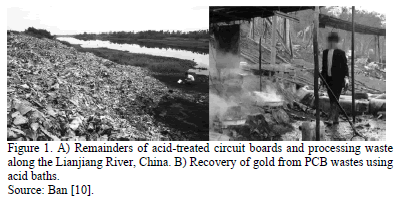
<body><![CDATA[<p><font size="3" face="Verdana, Arial, Helvetica, sans-serif"><b>1.  Introduction</b></font></p>     <p><font size="2" face="Verdana, Arial, Helvetica, sans-serif">Currently, there are a large number of products that   generate waste and significantly increase the volume of dumps and landfills due   to innovation by the electronic industry. Much of the waste generated   constitutes technological waste, whose recycling is being studied by several   authors, due to its social and environmental relevance. Among these wastes, one   of the most important are printed circuit boards (PCBs), which are the base of   the electronic industry.</font></p>     <p><font size="2" face="Verdana, Arial, Helvetica, sans-serif">PCBs constitute a kind of waste with difficult disposal   because their recycling is complex and expensive. The diversity of materials   and components present in them make their separation difficult. Separation of   electronic components and reusing of these materials require the removal of the   solder, which is a complex process. Also and for the majority of cases, such   components are unusable after that process due to the temperatures involved.</font></p>     <p><font size="2" face="Verdana, Arial, Helvetica, sans-serif">The PCBs construction process is currently migrating from   traditional eutectic Pb-Sn alloy to different lead-free alloys. This   replacement attempts to alleviate the problem </font></p>     <p><font size="2" face="Verdana, Arial, Helvetica, sans-serif">of Pb-Sn solder alloy, considered   toxic, but does not change the component separation problem for reuse and/or   recycling. Therefore, alternatives to the removal and disposal of these   materials without harming the environment become a new challenge. </font></p>     <p><font size="2" face="Verdana, Arial, Helvetica, sans-serif">The discarded PCBs have attracted public and researchers   attention &#91;1-9&#93;, since among their components there are toxic materials such as   heavy metals and brominated flame retardants (BFRs), causing enormous damage to   the environment if they are not properly treated (<a href="#fig01">Fig. 1</a>).</font></p>     <p align="center"><font size="2" face="Verdana, Arial, Helvetica, sans-serif"><a name="fig01"></a></font><img src="/img/revistas/dyna/v81n186/v81n186a20fig01.gif"></p>     <p><font size="2" face="Verdana, Arial, Helvetica, sans-serif">In general, PCB waste components can be divided into   metallic (MFs) and non-metallic fractions (NMF) &#91;11&#93;. NMF typical composition   comprises thermosetting resins (epoxy), glass fiber, plastics, reinforcement   materials, additives and other BFR, and constitute about 70wt-% of the PCB   wastes. Thermosetting resins cannot be recast or remodeled because of their molecular   structure and not recyclable &#91;11&#93;. The proportion of waste printed circuit   boards WPCBs in electronics waste is approximately 3% &#91;12,13&#93;.</font></p>     <p><font size="2" face="Verdana, Arial, Helvetica, sans-serif">Several authors &#91;1, 14-21&#93;, argue that WPCBs plastics   contain BFR, including polybrominated biphenyls (PBBs) and polybrominated   diphenyl ethers (PBDEs). Their combustion generates highly toxic gases, called   polybrominated dibenzodioxins and dibenzofurans, and dioxins and furans   (PCDF/Fs) and glass fiber significantly reduces fuel efficiency. Traditionally,   these nonmetallic materials are landfilled or incinerated resulting in wasted   resources and aggravating the environmental problem &#91;5, 22-26&#93;.</font></p>     <p><font size="2" face="Verdana, Arial, Helvetica, sans-serif">The metal fraction is comprised of ~16% of copper, ~4% of   tin-lead, ~3% of iron, ~2% of nickel, ~0.05% of silver, ~0.03% of gold, ~0.01%   palladium &#91;14,17, 27-30&#93; and even rare elements such as tantalum, covered or   mixed with various plastics and ceramics &#91;31&#93;. Li &#91;32&#93; states that the purity   of the precious metals in PCBs is 10 times higher than minerals rich in these   elements. Cui and Zhang &#91;33&#93; argue that the main economic objective for e-waste   recycling is the recovery of precious metals.</font></p>     ]]></body>
<body><![CDATA[<p><font size="2" face="Verdana, Arial, Helvetica, sans-serif">It is usually difficult and often confusing to quantify   the environmental consequences associated with materials, processes and   products. The difficulties are, for example, the determination of the   environmental effects associated with the objects of the comparison, the almost   impossible task of comparing different environmental effects and the amount of   data needed to compare related products. Sometimes, the necessary data are also   scarce or inaccessible, and then it is difficult to define the environmental   load analysis. Furthermore, the electronic industry is extremely large and   varied, characterized by long supply chains, and in the same way, indirect   environmental impacts associated to their products &#91;34&#93;.</font></p>     <p><font size="2" face="Verdana, Arial, Helvetica, sans-serif">There is a strong pressure from European companies not to   accept most electronic products with a tin-lead solder printed circuit board,   due to its toxicity. This type of welding is used, because of its easy   installation and use, but, since European laws became highly restrictive for   this type of material, it is important to study other types of welding, which   are less aggressive to the environment &#91;35&#93;.</font></p>     <p><font size="2" face="Verdana, Arial, Helvetica, sans-serif">Jie &#91;36&#93; argues that there is a growing environmental   awareness around the world. Therefore, an economically viable environmental   management system for the electro-electronic equipment end of life cycle is   necessary. It is very important for sustainable development, as the effective   cost and efficient environmental methods are needed to manage these wastes   &#91;29-30, 37-40&#93;.</font></p>     <p><font size="2" face="Verdana, Arial, Helvetica, sans-serif">According to Andrae &#91;34&#93; and other authors &#91;41-43&#93;, a   number of methods and tools related to environmental assessment, such as life   cycle assessment (LCA) and carbon footprint, were proposed in order to indicate   which alternative is better compared to others. Schematically, the life cycle   of a product consists of four stages: material extraction and processing,   manufacture, usage and end of life.</font></p>     <p><font size="2" face="Verdana, Arial, Helvetica, sans-serif">Griese et al. &#91;44&#93; argues that studies confirmed that lead   is the material with the greatest potential to be removed and had to be banned   to prevent uncontrolled releases; also, Pb-free alloys reduce the potential   environmental impact of electronics. This requires a complete LCA and detailed   study of the environmental performance of new materials substituents.</font></p>     <p><font size="2" face="Verdana, Arial, Helvetica, sans-serif">Some authors &#91;45-48&#93; realized that there is no simple replacement   for traditional welding. They indicate that the introduction of lead-free   solders reduces toxicity and potential risks in the electric-electronic waste   removal. But lead-free solders are less efficient in terms of resource and   energy consumption. Compared with traditional Sn-Pb solder, Pb-free materials   manufacturing doubles the cost in industries, increases energy use and promotes   the loss of valuable resources. In fact, Turbini et al. &#91;49&#93; recommend   increasing the conventional Pb-based electronics recycling, instead of   introducing lead-free solder. The main reason is to recycle copper in order to   reduce the environmental problems associated with its primary production and   mineral extraction.</font></p>     <p><font size="2" face="Verdana, Arial, Helvetica, sans-serif">Several studies are underway to reduce or completely eliminate   welding in printed circuit board manufacture. These alternatives provide   initial solutions to the problem, by reducing the use of soldering or replacing   the welding by another fastener such as a resin. However, they do not solve the   problem of separation. The ways in which electronic components are fixed in   PCBs still lacks adequate solutions. Therefore, fixing mechanisms used on a   printed circuit board are considered an open research topic.</font></p>     <p><font size="2" face="Verdana, Arial, Helvetica, sans-serif">Thus, this work reconsiders the alternatives for fixing the   components on printed circuit boards, through studying the supports used in   printed circuit boards, the existing types, properties and processes, seeking   to explore alternatives to traditional fixing (welding) in a printed circuit   board. Prototypes are made by mounting a board from established concepts and   making comparative tests of reliability, compared to conventionally fixed   boards for validation and providing a basis for future research.</font></p>     <p><font size="2" face="Verdana, Arial, Helvetica, sans-serif">The aim is to develop new alternatives and designs to   improve the fastening through alternative systems that facilitate assembly,   disassembly and maintenance of various components of the product during the   separation process, prior to recycling. Until now, there have been some initial   studies using prototypes for testing, including visual and functional testing.</font></p>     <p><font size="2" face="Verdana, Arial, Helvetica, sans-serif"><b>2.  Materials and   methods</b></font></p>     ]]></body>
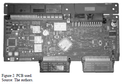
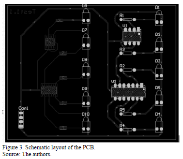
<body><![CDATA[<p><b><font size="2" face="Verdana, Arial, Helvetica, sans-serif">2.1.  Study of two   boards: Materials analysis    <br>   </font></b><font size="2" face="Verdana, Arial, Helvetica, sans-serif">The present analysis was performed for two printed circuit   boards regarding the percentage of each material, in order to evaluate the recycling   viability. This study was conducted with the cooperation of a PCBs   manufacturing company, located in the town of Valls (Tarragona-Barcelona) in   Spain, which provided the boards and the initial data (<a href="#fig02">Fig. 2</a>).</font></p>     <p align="center"><font size="2" face="Verdana, Arial, Helvetica, sans-serif"><a name="fig02"></a></font><img src="/img/revistas/dyna/v81n186/v81n186a20fig02.gif"></p>     <p><font size="2" face="Verdana, Arial, Helvetica, sans-serif"><b>2.2.  Fixing of   components by pressure</b>    <br>   </font><font size="2" face="Verdana, Arial, Helvetica, sans-serif">This work has applied for a patent with the INPI (National   Institute of Industrial Property of Brazil), with the name Production Process   of Printed Circuit Boards and the Resulting Product on 07/03/2013, number (BR   10 2013 005511 5).</font></p>     <p><font size="2" face="Verdana, Arial, Helvetica, sans-serif">The purpose of this study was to develop new methods for   attaching electronic components on a printed circuit board, through alternative   processes, and by selecting appropriate materials for these processes, aiming   to sustainability. Six initial conceptual designs were analyzed. The criteria   for the analysis were: mechanical fixing, electronic connection ability,   electrical conductivity, ease of assembly/disassembly, and low amount of   material used. In the present study, the component junctions were made by   pressure. Boards were fabricated to test the technical feasibility, analyzing   its initial run. The traditional process of manufacturing was maintained </font></p>     <p><font size="2" face="Verdana, Arial, Helvetica, sans-serif">with the addition of new steps   after the traditional ones, where a series of procedures was carried out to   make a board with fillets and holes adequate for mounting the electronic   circuit.</font></p>     <p><font size="2" face="Verdana, Arial, Helvetica, sans-serif">In this method of attachment, the board is made of two   parts, one with the printed circuit, which is pierced, and whose elements are   fixed by pressing on the other board; this does not require welding. The   contacts are made internally so that circuit designs are not visible. The   elements junction is performed by the two boards placed one on the other,   pressing the device and connections, and other items on the sides to further   secure the assembly.</font></p>     <p><font size="2" face="Verdana, Arial, Helvetica, sans-serif">For this set a simple circuit was designed (<a href="#fig03">Fig. 3</a>) to be   applied onto the board and the components to be fixed, in order to test the   proposal regarding the electrical resistance at each point of the fixed contact   elements, and therefore test the initial conceptual model feasibility. Virtual   and physical prototypes were performed. The next step was a functional   prototype building. For this prototype, a two-faced positive photosensitive   board was used, with dimensions of 100x160mm, made with fiberglass epoxy resin   (FR4), fire resistant insulation and covered with a conductive copper thin film   on both sides. A circuit with components for SMD (<i>Surface Mount Device</i>) and <i>Through-hole</i> were designed to test the two types that are currently used. 10 resistances (5   SMD and 5 <i>Through-hole</i>), 10 <i>Through-hole</i> LEDs, 10 &quot;chips&quot; (5 SMD and   5 <i>Through-hole</i>) and a battery   connected to the system to verify operation were used. After the traditional   steps to create a PCB were carried out, a series of procedures was performed   leading to a track with the same size of the board and the suitable holes for   mounting an electronic circuit.</font></p>     <p align="center"><font size="2" face="Verdana, Arial, Helvetica, sans-serif"><a name="fig03"></a></font><img src="/img/revistas/dyna/v81n186/v81n186a20fig03.gif"></p>     ]]></body>
<body><![CDATA[<p><font size="2" face="Verdana, Arial, Helvetica, sans-serif">In order to compare the proposed system with the   welding-fixed systems, three prototypes were fabricated using the same method:   The first prototype, with junctions of tin-lead (60Sn-40Pb), the second one,   lead-free welded (99.3 Sn-0.7Ag), and the third, with the previously described   junction method.</font></p>     <p><font size="2" face="Verdana, Arial, Helvetica, sans-serif"><b>2.3.  Tests   performed    <br>   </b></font><font size="2" face="Verdana, Arial, Helvetica, sans-serif">At this stage, prototypes were submitted to reliability,   visual and operating tests.</font></p>     <p><font size="2" face="Verdana, Arial, Helvetica, sans-serif"><b>2.3.1.  Visual test    <br>   </b></font><font size="2" face="Verdana, Arial, Helvetica, sans-serif">Visual analysis was performed as the first   characterization of prototypes. A visual inspection of the board can help to   identify and troubleshoot contacts.</font></p>     <p><font size="2" face="Verdana, Arial, Helvetica, sans-serif"><b>2.3.2.  Performance   test    <br>   </b></font><font size="2" face="Verdana, Arial, Helvetica, sans-serif">The performance test consists of checking the correct   operation of the board, determining the integrity of all electrical connections   and checking all LED points, in order to identify some damaged points and   components within the circuit in real working conditions.</font></p>     <p><font size="2" face="Verdana, Arial, Helvetica, sans-serif"><b>2.3.3.  Pending   tests</b>    <br>   </font><font size="2" face="Verdana, Arial, Helvetica, sans-serif">The following tests will be carried out in the   continuation of this work: Test of corrosion and humidity electric endurance   test and thermal-mechanical fatigue.</font></p>     <p>&nbsp;</p>     ]]></body>
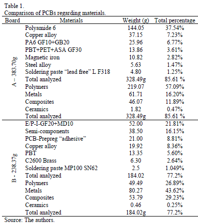
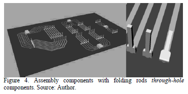
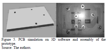
<body><![CDATA[<p><font size="3" face="Verdana, Arial, Helvetica, sans-serif"><b>3.  Results and   analysis</b></font></p>     <p><b><font size="2" face="Verdana, Arial, Helvetica, sans-serif">3.1.  Study of two   boards: Materials analysis    <br>   </font></b><font size="2" face="Verdana, Arial, Helvetica, sans-serif">The percentage of each material in these two printed   circuit projects was calculated from data provided by the company. In <a href="#tab01">Table 1</a>,   the composition of the materials with greater presence in the printed circuit board and a   comparison between the two boards studied, in relation to the percentage of the   materials, are shown.</font></p>     <p align="center"><font size="2" face="Verdana, Arial, Helvetica, sans-serif"><a name="tab01"></a></font><img src="/img/revistas/dyna/v81n186/v81n186a20tab01.gif"></p>     <p><font size="2" face="Verdana, Arial, Helvetica, sans-serif">There is a high weight percentage of polymeric materials.   Polyamide 6 is the material for the base of board. Also, there is the presence   of solder paste LF318 (Sn98.5/Ag1/Cu0.5) representing 1.25% of the total weight   of the printed circuit board. The main component of the solder, Sn, is a metal   component considered moderately toxic. In the second board there is a high   weight percentage of composite materials over other materials; the reinforced   glass fiber is the base material for the PCB</font></p>     <p><font size="2" face="Verdana, Arial, Helvetica, sans-serif">From <a href="#tab01">Table 1</a>, it can be seen that there is a great   difference in the amount of material used for the two boards. Each board   consists of a specific design for a particular use, so its components change   considerably. This indicates how difficult the identification and separation of   the materials can be, as well as the complexity of PCB recycling.</font></p>     <p><font size="2" face="Verdana, Arial, Helvetica, sans-serif"><b>3.2.  Fixing</b>    <br>   The physical and virtual prototypes of the first tests are   shown in <a href="#fig04">Fig.s 4</a>, <a href="#fig05">5</a> and <a href="#fig06">6</a>. The main objective of these prototypes is to test   the electrical resistance at each contact point between the fixed elements and,   therefore, to test the feasibility of the initial concept.</font></p>     <p align="center"><font size="2" face="Verdana, Arial, Helvetica, sans-serif"><a name="fig04"></a></font><img src="/img/revistas/dyna/v81n186/v81n186a20fig04.gif"></p>     <p align="center"><font size="2" face="Verdana, Arial, Helvetica, sans-serif"><a name="fig05"></a></font><img src="/img/revistas/dyna/v81n186/v81n186a20fig05.gif"></p>     ]]></body>
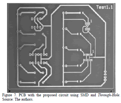
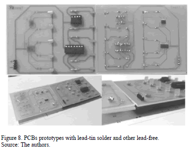
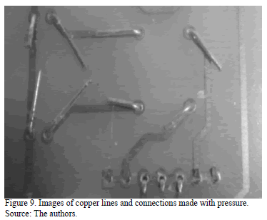
<body><![CDATA[<p align="center"><font size="2" face="Verdana, Arial, Helvetica, sans-serif"><a name="fig06"></a></font><img src="/img/revistas/dyna/v81n186/v81n186a20fig06.gif"></p>     <p><font size="2" face="Verdana, Arial, Helvetica, sans-serif">From the first prototype, a new circuit design with LEDs   was used to test the performance of the attachment system. <a href="#fig06">Fig. 6</a> shows the   virtual prototype and <a href="#fig07">Fig. 7</a>, the physical prototype. This circuit design is   more functional, simpler and with higher quality.</font></p>     <p align="center"><font size="2" face="Verdana, Arial, Helvetica, sans-serif"><a name="fig07"></a></font><img src="/img/revistas/dyna/v81n186/v81n186a20fig07.gif"></p>     <p><font size="2" face="Verdana, Arial, Helvetica, sans-serif">In <a href="#fig08">Fig. 8</a> the three prototypes appear in their respective   order, in order to compare different procedures and finishing of the boards.   The third prototype has the characteristic of not using welding for component   junctions, and hence facilitates disassembly and reuse of components; this   binding is non-permanent.</font></p>     <p align="center"><font size="2" face="Verdana, Arial, Helvetica, sans-serif"><a name="fig08"></a></font><img src="/img/revistas/dyna/v81n186/v81n186a20fig08.gif"></p>     <p><font size="2" face="Verdana, Arial, Helvetica, sans-serif"><b>3.3.  Tests results</b></font></p>     <p><b><font size="2" face="Verdana, Arial, Helvetica, sans-serif">3.3.1.  Visual test</font></b><font size="2" face="Verdana, Arial, Helvetica, sans-serif">    <br>   In this test copper lines and connections between the track   and the components were visually checked, seeking out possible errors. The   result showed that the defects were not detected visually in the system (<a href="#fig09">Fig.   9</a>).</font></p>     <p align="center"><font size="2" face="Verdana, Arial, Helvetica, sans-serif"><a name="fig09"></a></font><img src="/img/revistas/dyna/v81n186/v81n186a20fig09.gif"></p>     <p><font size="2" face="Verdana, Arial, Helvetica, sans-serif"><b>3.3.2.  Performance   test</b>    ]]></body>
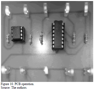
<body><![CDATA[<br>   </font><font size="2" face="Verdana, Arial, Helvetica, sans-serif">In this test, we examined the operation of the system   through the operation check on all connection points with the illumination of   the &quot;LEDs&quot;, shown in <a href="#fig10">Fig. 10</a>. Note that the LEDs were lighted due to   the pressure maintained in the system. The identification of this problem will   help to improve other prototypes.</font></p>     <p align="center"><font size="2" face="Verdana, Arial, Helvetica, sans-serif"><a name="fig10"></a></font><img src="/img/revistas/dyna/v81n186/v81n186a20fig10.gif"></p>     <p><font size="2" face="Verdana, Arial, Helvetica, sans-serif"><b>3.3.3.  Pending   tests</b>    <br>   </font><font size="2" face="Verdana, Arial, Helvetica, sans-serif">Prototypes will be developed with better quality and with   variations for comparison. The tests will be conducted in the ITT Fuse   (Technological Institute for Testing and Functional Safety) of the UNISINOS   (Universidade do Vale do Rio dos Sinos). Each prototype will perform an   operation analysis, visual analysis, analysis of the electrical resistance and   X-ray diffraction before and after the test. The tests to be performed will be   of thermal cycles, salt spray, thermal shock and vibration. </font></p>     <p>&nbsp;</p>     <p><font size="3" face="Verdana, Arial, Helvetica, sans-serif"><b>4.  Conclusion </b></font></p>     <p><font size="2" face="Verdana, Arial, Helvetica, sans-serif">There is a recent interest in the research of new   technologies for the recycling of printed circuit boards generated by the   growth of the electronics industry, which constitute an environmental problem   when they are disposed of, a subject which has been extensively studied. In   addition, regulations and laws in Europe have become stricter regarding   specifications of electronic components; therefore, it is necessary to conduct   further studies on the effects of these rules and laws in other countries.</font></p>     <p><font size="2" face="Verdana, Arial, Helvetica, sans-serif">Given the difficulty of recycling electronic wastes,   studies are focused on the development of techniques which facilitate the reuse   of these products and/or their components. The methods of fixing and joining of   components in the PCBs have become increasingly popular among researchers, with   a significant increase in studies of lead-free solders. However, it is   necessary to conduct studies related to alternatives to traditional processes   that do not yet have the attention of researchers and companies, and to take into   account the performance of the final product (LCA), through integrated   approaches in terms of processes, materials and technologies.</font></p>     <p><font size="2" face="Verdana, Arial, Helvetica, sans-serif">The idea of eliminating the use of welding is not new, but   the methods previously proposed (for example, replacement with conductive   adhesive) have not been accepted by the market, presumably due to operating   difficulties or unreliability. Only a few works exist which propose   alternatives to the traditional procedure.</font></p>     <p><font size="2" face="Verdana, Arial, Helvetica, sans-serif">This initial study is essential to guide new research,   generate alternatives and test them for specific applications. Currently, ways   in which the electronic components are fixed to printed circuit boards still   lack suitable alternatives to replace them. Therefore, an alternative fixing   PCBs was proposed, and tested and compared with traditional forms. The first   performance test showed positive results with regard to the operation of the   circuit elements. The prototypes were hand-made and showed reasonable quality.   Better quality is expected in later works, due to prior knowledge of the   construction and operation of the first prototype.</font></p>     ]]></body>
<body><![CDATA[<p>&nbsp;</p>     <p><font size="3" face="Verdana, Arial, Helvetica, sans-serif"><b>Acknowledgements</b></font></p>     <p><font size="2" face="Verdana, Arial, Helvetica, sans-serif">The authors wish to acknowledge the financial support of   CAPES (Brazilian Government Agency for Human Resources Development), CNPq   (Brazilian National Council for Scientific and Technological Development) and   the Euro Brazilian Windows II Project (EBW II).</font></p>     <p>&nbsp;</p>     <p><font size="3" face="Verdana, Arial, Helvetica, sans-serif"><b>References</b></font></p>     <!-- ref --><p><font size="2" face="Verdana, Arial, Helvetica, sans-serif"><b>&#91;1&#93;</b>.&nbsp; Cui, J. and Forssberg, E., Mechanical recycling of waste electric and   electronic equipment: A review. Journal of Hazardous Materials, 99, pp. 243-263,   2003.    &nbsp;&nbsp;&nbsp;&nbsp;&nbsp;&nbsp;&nbsp;&nbsp;[&#160;<a href="javascript:void(0);" onclick="javascript: window.open('/scielo.php?script=sci_nlinks&ref=000098&pid=S0012-7353201400040002000001&lng=','','width=640,height=500,resizable=yes,scrollbars=1,menubar=yes,');">Links</a>&#160;]<!-- end-ref --></font></p>     <!-- ref --><p><font size="2" face="Verdana, Arial, Helvetica, sans-serif"><b>&#91;2&#93;</b>.&nbsp; AEA TECHNOLOGY: WEEE &amp; Hazardous Waste, A report produced for DEFRA.   Aea, 2004.    &nbsp;&nbsp;&nbsp;&nbsp;&nbsp;&nbsp;&nbsp;&nbsp;[&#160;<a href="javascript:void(0);" onclick="javascript: window.open('/scielo.php?script=sci_nlinks&ref=000100&pid=S0012-7353201400040002000002&lng=','','width=640,height=500,resizable=yes,scrollbars=1,menubar=yes,');">Links</a>&#160;]<!-- end-ref --></font></p>     <!-- ref --><p><font size="2" face="Verdana, Arial, Helvetica, sans-serif"><b>&#91;3&#93;</b>.&nbsp; Wang, D., Cai, Z., Jiang, G., Leung, A., Wong, M. H. and Wong, W. K.,   Determination of polybrominated diphenyl ethers in soil and sediment from an   electronic waste recycling facility. Chemosphere, 60, pp. 810-816, 2005.    &nbsp;&nbsp;&nbsp;&nbsp;&nbsp;&nbsp;&nbsp;&nbsp;[&#160;<a href="javascript:void(0);" onclick="javascript: window.open('/scielo.php?script=sci_nlinks&ref=000102&pid=S0012-7353201400040002000003&lng=','','width=640,height=500,resizable=yes,scrollbars=1,menubar=yes,');">Links</a>&#160;]<!-- end-ref --></font></p>     <!-- ref --><p><font size="2" face="Verdana, Arial, Helvetica, sans-serif"><b>&#91;4&#93;</b>.&nbsp; EPS CANADA, Electronics Product Stewardship Canada: Environmentally   Sound Recycling of Electronics. Guidance document, Canada, EPS 2006.    &nbsp;&nbsp;&nbsp;&nbsp;&nbsp;&nbsp;&nbsp;&nbsp;[&#160;<a href="javascript:void(0);" onclick="javascript: window.open('/scielo.php?script=sci_nlinks&ref=000104&pid=S0012-7353201400040002000004&lng=','','width=640,height=500,resizable=yes,scrollbars=1,menubar=yes,');">Links</a>&#160;]<!-- end-ref --></font></p>     <!-- ref --><p><font size="2" face="Verdana, Arial, Helvetica, sans-serif"><b>&#91;5&#93;</b>.&nbsp; Owens, C.V., Lambright, C., Bobseine, K., Ryan, B., Gray Jr., R. E.,   Gullett, B. K. and Wilson, V. S., Identification of estrogenic compounds   emitted from the combustion of computer printed circuit boards in electronic   waste. Environmental Science and Technology, 41, pp. 8506-8511, 2007.    &nbsp;&nbsp;&nbsp;&nbsp;&nbsp;&nbsp;&nbsp;&nbsp;[&#160;<a href="javascript:void(0);" onclick="javascript: window.open('/scielo.php?script=sci_nlinks&ref=000106&pid=S0012-7353201400040002000005&lng=','','width=640,height=500,resizable=yes,scrollbars=1,menubar=yes,');">Links</a>&#160;]<!-- end-ref --></font></p>     <!-- ref --><p><font size="2" face="Verdana, Arial, Helvetica, sans-serif"><b>&#91;6&#93;</b>.&nbsp; Leung, A. O. W., Duzgoren-Aydin, N. S., Cheung, K. C. and Wong, M. H.,   Heavy metals concentrations of surface dust frome-waste recycling and its human   health implications in Southeast China. Environmental Science and Technology,   42, pp. 2674-2680, 2008.    &nbsp;&nbsp;&nbsp;&nbsp;&nbsp;&nbsp;&nbsp;&nbsp;[&#160;<a href="javascript:void(0);" onclick="javascript: window.open('/scielo.php?script=sci_nlinks&ref=000108&pid=S0012-7353201400040002000006&lng=','','width=640,height=500,resizable=yes,scrollbars=1,menubar=yes,');">Links</a>&#160;]<!-- end-ref --></font></p>     <!-- ref --><p><font size="2" face="Verdana, Arial, Helvetica, sans-serif"><b>&#91;7&#93;</b>.&nbsp; Vasile, C., Brebu, M.A., Totolin, M., Yanik, J. Karayildirim, T. and Darie,   H., Feedstock recycling from the printed circuit boards of used computers.   Energy Fuel, 22, pp. 1658-1665, 2008.    &nbsp;&nbsp;&nbsp;&nbsp;&nbsp;&nbsp;&nbsp;&nbsp;[&#160;<a href="javascript:void(0);" onclick="javascript: window.open('/scielo.php?script=sci_nlinks&ref=000110&pid=S0012-7353201400040002000007&lng=','','width=640,height=500,resizable=yes,scrollbars=1,menubar=yes,');">Links</a>&#160;]<!-- end-ref --></font></p>     <!-- ref --><p><font size="2" face="Verdana, Arial, Helvetica, sans-serif"><b>&#91;8&#93;</b>.&nbsp; Sep&uacute;lveda, A., Schuluep, M., Renaud, F. G., Streicher, M., Kuehr, R.,   Hagelüken, C. and Gerecke, A. C., A review of the environmental fate and   effects of hazardous substances released from electrical and electronic   equipments during recycling: Examples from China and India. Environmental   Impact Assessment Reviews, 30, pp. 28-41, 2010.    &nbsp;&nbsp;&nbsp;&nbsp;&nbsp;&nbsp;&nbsp;&nbsp;[&#160;<a href="javascript:void(0);" onclick="javascript: window.open('/scielo.php?script=sci_nlinks&ref=000112&pid=S0012-7353201400040002000008&lng=','','width=640,height=500,resizable=yes,scrollbars=1,menubar=yes,');">Links</a>&#160;]<!-- end-ref --></font></p>     <!-- ref --><p><font size="2" face="Verdana, Arial, Helvetica, sans-serif"><b>&#91;9&#93;</b>.&nbsp; Zhou, Y. and Qiu, K., A new technology for recycling materials from   waste printed circuit boards. Journal of Hazardous Materials, 175, pp. 823-828,   2010.    &nbsp;&nbsp;&nbsp;&nbsp;&nbsp;&nbsp;&nbsp;&nbsp;[&#160;<a href="javascript:void(0);" onclick="javascript: window.open('/scielo.php?script=sci_nlinks&ref=000114&pid=S0012-7353201400040002000009&lng=','','width=640,height=500,resizable=yes,scrollbars=1,menubar=yes,');">Links</a>&#160;]<!-- end-ref --></font></p>     <!-- ref --><p><font size="2" face="Verdana, Arial, Helvetica, sans-serif"><b>&#91;10&#93;</b>.&nbsp; BAN, Exporting Harm: The High-Tech-Trashing of Asia, SVTC. Availaible: <a href="http://www.ban.org/e-waste/technotrashfinalcomp.pdf" target="_blank">http://www.ban.org/e-waste/technotrashfinalcomp.pdf</a> &#91; Cited 15 May 2013 &#93;    &nbsp;&nbsp;&nbsp;&nbsp;&nbsp;&nbsp;&nbsp;&nbsp;[&#160;<a href="javascript:void(0);" onclick="javascript: window.open('/scielo.php?script=sci_nlinks&ref=000116&pid=S0012-7353201400040002000010&lng=','','width=640,height=500,resizable=yes,scrollbars=1,menubar=yes,');">Links</a>&#160;]<!-- end-ref -->.</font></p>     <!-- ref --><p><font size="2" face="Verdana, Arial, Helvetica, sans-serif"><b>&#91;11&#93;</b>.&nbsp; Guo, J., Guo, J. and Xu, Z., Recycling of non-metallic fractions from   waste printed circuit boards: A review, Journal of Hazardous Materials, 168   (2-3), pp. 567-590, 2009.    &nbsp;&nbsp;&nbsp;&nbsp;&nbsp;&nbsp;&nbsp;&nbsp;[&#160;<a href="javascript:void(0);" onclick="javascript: window.open('/scielo.php?script=sci_nlinks&ref=000118&pid=S0012-7353201400040002000011&lng=','','width=640,height=500,resizable=yes,scrollbars=1,menubar=yes,');">Links</a>&#160;]<!-- end-ref --></font></p>     <!-- ref --><p><font size="2" face="Verdana, Arial, Helvetica, sans-serif"><b>&#91;12&#93;</b>.&nbsp; Bernardes, A., Bohlinger, I. and Rodriguez, D., Recycling of printed   circuit boards by melting with oxidising/reducing top blowing process. In: B.   Mishra (Ed.), Proceedings of Sessions and Symposia Sponsored by the Extraction   and Processing Division, TMS Annual Meeting, Orlando, FL, USA, 1997, pp. 363-375.    &nbsp;&nbsp;&nbsp;&nbsp;&nbsp;&nbsp;&nbsp;&nbsp;[&#160;<a href="javascript:void(0);" onclick="javascript: window.open('/scielo.php?script=sci_nlinks&ref=000120&pid=S0012-7353201400040002000012&lng=','','width=640,height=500,resizable=yes,scrollbars=1,menubar=yes,');">Links</a>&#160;]<!-- end-ref --></font></p>     <!-- ref --><p><font size="2" face="Verdana, Arial, Helvetica, sans-serif"><b>&#91;13&#93;</b>.&nbsp; Basdere, B. and Seliger, G., Disassembly factories for electrical and   electronic products to recover resources in product and material cycles,   Environmental Science and Technology, 37, pp. 5354-5362, 2003.    &nbsp;&nbsp;&nbsp;&nbsp;&nbsp;&nbsp;&nbsp;&nbsp;[&#160;<a href="javascript:void(0);" onclick="javascript: window.open('/scielo.php?script=sci_nlinks&ref=000122&pid=S0012-7353201400040002000013&lng=','','width=640,height=500,resizable=yes,scrollbars=1,menubar=yes,');">Links</a>&#160;]<!-- end-ref --></font></p>     <!-- ref --><p><font size="2" face="Verdana, Arial, Helvetica, sans-serif"><b>&#91;14&#93;</b>.&nbsp; Richter, H., Lorenz, W. and Bahadir, M., Examination of organic and   inorganic xenobiotics in equipped printed circuits, Chemosphere, 35, pp. 169-179,   1997.    &nbsp;&nbsp;&nbsp;&nbsp;&nbsp;&nbsp;&nbsp;&nbsp;[&#160;<a href="javascript:void(0);" onclick="javascript: window.open('/scielo.php?script=sci_nlinks&ref=000124&pid=S0012-7353201400040002000014&lng=','','width=640,height=500,resizable=yes,scrollbars=1,menubar=yes,');">Links</a>&#160;]<!-- end-ref --></font></p>     <!-- ref --><p><font size="2" face="Verdana, Arial, Helvetica, sans-serif"><b>&#91;15&#93;</b>.&nbsp; Menad, N., Bjorkman, B. and Allain, E.G., Combustion of plastics   contained in electric and electronic scrap, Resources, Conservation and Recycling, 24, pp. 65-85, 1998.    &nbsp;&nbsp;&nbsp;&nbsp;&nbsp;&nbsp;&nbsp;&nbsp;[&#160;<a href="javascript:void(0);" onclick="javascript: window.open('/scielo.php?script=sci_nlinks&ref=000126&pid=S0012-7353201400040002000015&lng=','','width=640,height=500,resizable=yes,scrollbars=1,menubar=yes,');">Links</a>&#160;]<!-- end-ref --></font></p>     <!-- ref --><p><font size="2" face="Verdana, Arial, Helvetica, sans-serif"><b>&#91;16&#93;</b>.&nbsp; Riess, M., Ernst, T., Popp, R., Müller, B., Thoma, H., Vierle, O., Wolf,   M. and Van Eldik, R., Analysis of flame retarded polymers and recycling   materials, Chemosphere, 40, 937-941, 2000.    &nbsp;&nbsp;&nbsp;&nbsp;&nbsp;&nbsp;&nbsp;&nbsp;[&#160;<a href="javascript:void(0);" onclick="javascript: window.open('/scielo.php?script=sci_nlinks&ref=000128&pid=S0012-7353201400040002000016&lng=','','width=640,height=500,resizable=yes,scrollbars=1,menubar=yes,');">Links</a>&#160;]<!-- end-ref --></font></p>     <!-- ref --><p><font size="2" face="Verdana, Arial, Helvetica, sans-serif"><b>&#91;17&#93;</b>.&nbsp; Vehlow, J., Bergfeldt, B., Jay, K., Hunsinger, H. and Mark, F.E.,   Thermal treatment of electrical and electronic waste plastics, Waste Management   &amp; Research. 18, 131-140, 2000.    &nbsp;&nbsp;&nbsp;&nbsp;&nbsp;&nbsp;&nbsp;&nbsp;[&#160;<a href="javascript:void(0);" onclick="javascript: window.open('/scielo.php?script=sci_nlinks&ref=000130&pid=S0012-7353201400040002000017&lng=','','width=640,height=500,resizable=yes,scrollbars=1,menubar=yes,');">Links</a>&#160;]<!-- end-ref --></font></p>     <!-- ref --><p><font size="2" face="Verdana, Arial, Helvetica, sans-serif"><b>&#91;18&#93;</b>.&nbsp; Ebert, J. and Bahadir, M., Formation of PBDD/F from flame-retarded   plastic materials under thermal stress, Environmental International, 29, pp. 711-716,   2003.    &nbsp;&nbsp;&nbsp;&nbsp;&nbsp;&nbsp;&nbsp;&nbsp;[&#160;<a href="javascript:void(0);" onclick="javascript: window.open('/scielo.php?script=sci_nlinks&ref=000132&pid=S0012-7353201400040002000018&lng=','','width=640,height=500,resizable=yes,scrollbars=1,menubar=yes,');">Links</a>&#160;]<!-- end-ref --></font></p>     <!-- ref --><p><font size="2" face="Verdana, Arial, Helvetica, sans-serif"><b>&#91;19&#93;</b>.&nbsp; Schlummer, M., Gruber, L., Mäurer, A., Wolz, G. and Van Eldik, R.,   Characterization of polymer fractions from waste electrical and electronic   equipment (WEEE) and implications for waste management, Chemosphere, 67,   1866-1876, 2007.    &nbsp;&nbsp;&nbsp;&nbsp;&nbsp;&nbsp;&nbsp;&nbsp;[&#160;<a href="javascript:void(0);" onclick="javascript: window.open('/scielo.php?script=sci_nlinks&ref=000134&pid=S0012-7353201400040002000019&lng=','','width=640,height=500,resizable=yes,scrollbars=1,menubar=yes,');">Links</a>&#160;]<!-- end-ref --></font></p>     <!-- ref --><p><font size="2" face="Verdana, Arial, Helvetica, sans-serif"><b>&#91;20&#93;</b>.&nbsp; Dimitrakakis, E., Janz, A., Bilitewski, B. and Gidarakos, E., Small   WEEE: determining recyclables and hazardous substances in plastics, Journal of   Hazardous Materials, 161, pp. 913-919, 2008.    &nbsp;&nbsp;&nbsp;&nbsp;&nbsp;&nbsp;&nbsp;&nbsp;[&#160;<a href="javascript:void(0);" onclick="javascript: window.open('/scielo.php?script=sci_nlinks&ref=000136&pid=S0012-7353201400040002000020&lng=','','width=640,height=500,resizable=yes,scrollbars=1,menubar=yes,');">Links</a>&#160;]<!-- end-ref --> </font></p>     <!-- ref --><p><font size="2" face="Verdana, Arial, Helvetica, sans-serif"><b>&#91;21&#93;</b>.&nbsp; Taurino, R., Pozzi, P. and Zanasi, T., Facile characterization of   polymer fractions from waste electrical and electronic equipment (WEEE) for   mechanical recycling, Journal of Waste Management, 30, pp. 2601-2607, 2010.    &nbsp;&nbsp;&nbsp;&nbsp;&nbsp;&nbsp;&nbsp;&nbsp;[&#160;<a href="javascript:void(0);" onclick="javascript: window.open('/scielo.php?script=sci_nlinks&ref=000138&pid=S0012-7353201400040002000021&lng=','','width=640,height=500,resizable=yes,scrollbars=1,menubar=yes,');">Links</a>&#160;]<!-- end-ref --></font></p>     <!-- ref --><p><font size="2" face="Verdana, Arial, Helvetica, sans-serif"><b>&#91;22&#93;</b>.&nbsp; Rotter, S., Schwermetalle in Haushaltsabfällen (Heavy Metals in   Household Waste), Doctoral Thesis, Edited by Forum für Abfallwirtschaft und   Altlasten e.V.Pirna, Germany, 2002.    &nbsp;&nbsp;&nbsp;&nbsp;&nbsp;&nbsp;&nbsp;&nbsp;[&#160;<a href="javascript:void(0);" onclick="javascript: window.open('/scielo.php?script=sci_nlinks&ref=000140&pid=S0012-7353201400040002000022&lng=','','width=640,height=500,resizable=yes,scrollbars=1,menubar=yes,');">Links</a>&#160;]<!-- end-ref --></font></p>     <!-- ref --><p><font size="2" face="Verdana, Arial, Helvetica, sans-serif"><b>&#91;23&#93;</b>.&nbsp; Jang, Y. C. and Townsend, T. G., Leaching of lead from computer printed   wire boards and cathode ray tubes by municipal solid waste landfill leachates,   Environmental Science and Technology, 37, pp. 4778-4784, 2003.    &nbsp;&nbsp;&nbsp;&nbsp;&nbsp;&nbsp;&nbsp;&nbsp;[&#160;<a href="javascript:void(0);" onclick="javascript: window.open('/scielo.php?script=sci_nlinks&ref=000142&pid=S0012-7353201400040002000023&lng=','','width=640,height=500,resizable=yes,scrollbars=1,menubar=yes,');">Links</a>&#160;]<!-- end-ref --></font></p>     <!-- ref --><p><font size="2" face="Verdana, Arial, Helvetica, sans-serif"><b>&#91;24&#93;</b>.&nbsp; Hagelüken, C., Improving metal returns and eco-efficiency in electronics   recycling - a holistic approach for interface optimization between   preprocessing and integrated metals smelting and refining, In: Proceedings of   IEEE International Symposium on Electronics and the Environment, San Francisco,   USA, 2006, pp. 218-223.    &nbsp;&nbsp;&nbsp;&nbsp;&nbsp;&nbsp;&nbsp;&nbsp;[&#160;<a href="javascript:void(0);" onclick="javascript: window.open('/scielo.php?script=sci_nlinks&ref=000144&pid=S0012-7353201400040002000024&lng=','','width=640,height=500,resizable=yes,scrollbars=1,menubar=yes,');">Links</a>&#160;]<!-- end-ref --></font></p>     <!-- ref --><p><font size="2" face="Verdana, Arial, Helvetica, sans-serif"><b>&#91;25&#93;</b>.&nbsp; Huang, Y., Takaoka, M., Takeda, N. and Oshita, K., Partial removal of   PCDD/Fs, coplanar PCBs, and PCBs from municipal solid waste incineration fly ash   by a column flotation process, Environmental Science and Technology, 41, pp. 257-262,   2007.    &nbsp;&nbsp;&nbsp;&nbsp;&nbsp;&nbsp;&nbsp;&nbsp;[&#160;<a href="javascript:void(0);" onclick="javascript: window.open('/scielo.php?script=sci_nlinks&ref=000146&pid=S0012-7353201400040002000025&lng=','','width=640,height=500,resizable=yes,scrollbars=1,menubar=yes,');">Links</a>&#160;]<!-- end-ref --></font></p>     <!-- ref --><p><font size="2" face="Verdana, Arial, Helvetica, sans-serif"><b>&#91;26&#93;</b>.&nbsp; Janz, A., Rotter, V. S. and Bilitewski, B., Transfer of heavy metals   released by WEEE and batteries into the high caloric fraction during   MBT-processes, In: Proceedings of First International Conference on Hazardous   Waste Management, Chania, Greece, 2008, 5 P.    &nbsp;&nbsp;&nbsp;&nbsp;&nbsp;&nbsp;&nbsp;&nbsp;[&#160;<a href="javascript:void(0);" onclick="javascript: window.open('/scielo.php?script=sci_nlinks&ref=000148&pid=S0012-7353201400040002000026&lng=','','width=640,height=500,resizable=yes,scrollbars=1,menubar=yes,');">Links</a>&#160;]<!-- end-ref --></font></p>     <!-- ref --><p><font size="2" face="Verdana, Arial, Helvetica, sans-serif"><b>&#91;27&#93;</b>.&nbsp; Iji, M. and Yokoyama, S., Recycling of printed wiring boards with   mounted electronic components, Circuit World, 23, pp. 10-15, 1997.    &nbsp;&nbsp;&nbsp;&nbsp;&nbsp;&nbsp;&nbsp;&nbsp;[&#160;<a href="javascript:void(0);" onclick="javascript: window.open('/scielo.php?script=sci_nlinks&ref=000150&pid=S0012-7353201400040002000027&lng=','','width=640,height=500,resizable=yes,scrollbars=1,menubar=yes,');">Links</a>&#160;]<!-- end-ref --></font></p>     <!-- ref --><p><font size="2" face="Verdana, Arial, Helvetica, sans-serif"><b>&#91;28&#93;</b>.&nbsp; Ernst, T., Popp, R. and Van Eldik, R., Quantification of heavy metals   for the recycling of waste plastics from electrotechnical applications,   Talanta, 53, 347-357, 2000.    &nbsp;&nbsp;&nbsp;&nbsp;&nbsp;&nbsp;&nbsp;&nbsp;[&#160;<a href="javascript:void(0);" onclick="javascript: window.open('/scielo.php?script=sci_nlinks&ref=000152&pid=S0012-7353201400040002000028&lng=','','width=640,height=500,resizable=yes,scrollbars=1,menubar=yes,');">Links</a>&#160;]<!-- end-ref --></font></p>     <!-- ref --><p><font size="2" face="Verdana, Arial, Helvetica, sans-serif"><b>&#91;29&#93;</b>.&nbsp; Veit, M. H., Pereira, C. D. C. and Bernardes, A. M., Using mechanical   processing in recycling printed wiring boards, JOM, 54, pp. 45-47, 2002.    &nbsp;&nbsp;&nbsp;&nbsp;&nbsp;&nbsp;&nbsp;&nbsp;[&#160;<a href="javascript:void(0);" onclick="javascript: window.open('/scielo.php?script=sci_nlinks&ref=000154&pid=S0012-7353201400040002000029&lng=','','width=640,height=500,resizable=yes,scrollbars=1,menubar=yes,');">Links</a>&#160;]<!-- end-ref --></font></p>     <!-- ref --><p><font size="2" face="Verdana, Arial, Helvetica, sans-serif"><b>&#91;30&#93;</b>.&nbsp; Goosey, M. and Kellner, R., Recycling technologies for the treatment of   end of life printed circuit boards (PCBs), Circuit World, 29, pp. 33-37, 2003.    &nbsp;&nbsp;&nbsp;&nbsp;&nbsp;&nbsp;&nbsp;&nbsp;[&#160;<a href="javascript:void(0);" onclick="javascript: window.open('/scielo.php?script=sci_nlinks&ref=000156&pid=S0012-7353201400040002000030&lng=','','width=640,height=500,resizable=yes,scrollbars=1,menubar=yes,');">Links</a>&#160;]<!-- end-ref --></font></p>     <!-- ref --><p><font size="2" face="Verdana, Arial, Helvetica, sans-serif"><b>&#91;31&#93;</b>.&nbsp; Hoffmann, J. E., Recovering precious metals from electronic scrap, JOM,.   44, pp. 43-48, 1992.    &nbsp;&nbsp;&nbsp;&nbsp;&nbsp;&nbsp;&nbsp;&nbsp;[&#160;<a href="javascript:void(0);" onclick="javascript: window.open('/scielo.php?script=sci_nlinks&ref=000158&pid=S0012-7353201400040002000031&lng=','','width=640,height=500,resizable=yes,scrollbars=1,menubar=yes,');">Links</a>&#160;]<!-- end-ref --></font></p>     <!-- ref --><p><font size="2" face="Verdana, Arial, Helvetica, sans-serif"><b>&#91;32&#93;</b>.&nbsp; Li, J., Shirivastava, P., Gao, Z. and Zhang, H., Printed circuit board   recycling: a state of the-art survey, Electronics Packaging Manufacturing, IEEE   Transactions on, 27, pp. 33-42, 2004.    &nbsp;&nbsp;&nbsp;&nbsp;&nbsp;&nbsp;&nbsp;&nbsp;[&#160;<a href="javascript:void(0);" onclick="javascript: window.open('/scielo.php?script=sci_nlinks&ref=000160&pid=S0012-7353201400040002000032&lng=','','width=640,height=500,resizable=yes,scrollbars=1,menubar=yes,');">Links</a>&#160;]<!-- end-ref --></font></p>     <!-- ref --><p><font size="2" face="Verdana, Arial, Helvetica, sans-serif"><b>&#91;33&#93;</b>.&nbsp; Cui, J. and Zhang, L., Metallurgical recovery of metals from electronic   waste: A review, Journal of Hazardous Materials, 158, pp. 228-256. 2008.    &nbsp;&nbsp;&nbsp;&nbsp;&nbsp;&nbsp;&nbsp;&nbsp;[&#160;<a href="javascript:void(0);" onclick="javascript: window.open('/scielo.php?script=sci_nlinks&ref=000162&pid=S0012-7353201400040002000033&lng=','','width=640,height=500,resizable=yes,scrollbars=1,menubar=yes,');">Links</a>&#160;]<!-- end-ref --></font></p>     <!-- ref --><p><font size="2" face="Verdana, Arial, Helvetica, sans-serif"><b>&#91;34&#93;</b>.&nbsp; Andrae, A. S. G., Global life cycle impact assesments of material   shifts: The example of a Lead-free electronics industry, Springer. Hardcover.   183 P., 2010.    &nbsp;&nbsp;&nbsp;&nbsp;&nbsp;&nbsp;&nbsp;&nbsp;[&#160;<a href="javascript:void(0);" onclick="javascript: window.open('/scielo.php?script=sci_nlinks&ref=000164&pid=S0012-7353201400040002000034&lng=','','width=640,height=500,resizable=yes,scrollbars=1,menubar=yes,');">Links</a>&#160;]<!-- end-ref --></font></p>     <!-- ref --><p><font size="2" face="Verdana, Arial, Helvetica, sans-serif"><b>&#91;35&#93;</b>.&nbsp; Nogueira, C. L. A., Queiroz-Neto, J. P. and Manzato,   L. O., Impacto do uso de solda <i>lead-free</i> no processo de tecnologia de montagem em superf&iacute;cie (SMT), II Congresso de   Pesquisa e Inovação da Rede Norte Nordeste de Educação Tecnol&oacute;gica. João Pessoa   - PB,Brasilm  2007.    &nbsp;&nbsp;&nbsp;&nbsp;&nbsp;&nbsp;&nbsp;&nbsp;[&#160;<a href="javascript:void(0);" onclick="javascript: window.open('/scielo.php?script=sci_nlinks&ref=000166&pid=S0012-7353201400040002000035&lng=','','width=640,height=500,resizable=yes,scrollbars=1,menubar=yes,');">Links</a>&#160;]<!-- end-ref --></font></p>     <!-- ref --><p><font size="2" face="Verdana, Arial, Helvetica, sans-serif"><b>&#91;36&#93;</b>.&nbsp; Jie, G., Ying-Shum, L. and Mai-Xi, L., Product characterization of waste   printed circuit board by pyrolysis, Journal of Analytical and Applied Pyrolysis,   83, pp. 185-189, 2008.    &nbsp;&nbsp;&nbsp;&nbsp;&nbsp;&nbsp;&nbsp;&nbsp;[&#160;<a href="javascript:void(0);" onclick="javascript: window.open('/scielo.php?script=sci_nlinks&ref=000168&pid=S0012-7353201400040002000036&lng=','','width=640,height=500,resizable=yes,scrollbars=1,menubar=yes,');">Links</a>&#160;]<!-- end-ref --></font></p>     <!-- ref --><p><font size="2" face="Verdana, Arial, Helvetica, sans-serif"><b>&#91;37&#93;</b>.&nbsp; Zong, G., Jianzhi, L. and Hong, C. Z., Printed circuit board recycling:   a state-of art survey. Proceedings IEEE International Symposium on Electronics   and the Environment, pp. 234-241, 2002.    &nbsp;&nbsp;&nbsp;&nbsp;&nbsp;&nbsp;&nbsp;&nbsp;[&#160;<a href="javascript:void(0);" onclick="javascript: window.open('/scielo.php?script=sci_nlinks&ref=000170&pid=S0012-7353201400040002000037&lng=','','width=640,height=500,resizable=yes,scrollbars=1,menubar=yes,');">Links</a>&#160;]<!-- end-ref --></font></p>     <!-- ref --><p><font size="2" face="Verdana, Arial, Helvetica, sans-serif"><b>&#91;38&#93;</b>.&nbsp; Kang, H. Y. and Schoenung, J. M., Electronic waste recycling: A review   of U.S. infrastructure and technology options, Resources, Conservation and Recycling, 45, 368-400, 2005.    &nbsp;&nbsp;&nbsp;&nbsp;&nbsp;&nbsp;&nbsp;&nbsp;[&#160;<a href="javascript:void(0);" onclick="javascript: window.open('/scielo.php?script=sci_nlinks&ref=000172&pid=S0012-7353201400040002000038&lng=','','width=640,height=500,resizable=yes,scrollbars=1,menubar=yes,');">Links</a>&#160;]<!-- end-ref --></font></p>     <!-- ref --><p><font size="2" face="Verdana, Arial, Helvetica, sans-serif"><b>&#91;39&#93;</b>.&nbsp; Sinha-Khetriwala, D., Kraeuchib, P. and Schwaninger, M. A., Comparison   of electronic waste recycling in Switzerland and in India, Journal of Environmental   Impact Assessment Reviews, 25, pp. 492-504, 2005.    &nbsp;&nbsp;&nbsp;&nbsp;&nbsp;&nbsp;&nbsp;&nbsp;[&#160;<a href="javascript:void(0);" onclick="javascript: window.open('/scielo.php?script=sci_nlinks&ref=000174&pid=S0012-7353201400040002000039&lng=','','width=640,height=500,resizable=yes,scrollbars=1,menubar=yes,');">Links</a>&#160;]<!-- end-ref --></font></p>     <!-- ref --><p><font size="2" face="Verdana, Arial, Helvetica, sans-serif"><b>&#91;40&#93;</b>.&nbsp; Eswaraiah, C., Kavitha, T., Vidyasagar, S. and Narayana, S.,   Classification of metals and plastics from printed circuit boards (PCB) using   air classifier, Chemical Engineering and Processing: Process Intensification, 47,   565-576, 2008.    &nbsp;&nbsp;&nbsp;&nbsp;&nbsp;&nbsp;&nbsp;&nbsp;[&#160;<a href="javascript:void(0);" onclick="javascript: window.open('/scielo.php?script=sci_nlinks&ref=000176&pid=S0012-7353201400040002000040&lng=','','width=640,height=500,resizable=yes,scrollbars=1,menubar=yes,');">Links</a>&#160;]<!-- end-ref --></font></p>     <!-- ref --><p><font size="2" face="Verdana, Arial, Helvetica, sans-serif"><b>&#91;41&#93;</b>.&nbsp; Botin, J. A., Integrating   sustainability down to the operational levels of a mining company, DYNA, 77   (161), pp. 43-49, 2010.    &nbsp;&nbsp;&nbsp;&nbsp;&nbsp;&nbsp;&nbsp;&nbsp;[&#160;<a href="javascript:void(0);" onclick="javascript: window.open('/scielo.php?script=sci_nlinks&ref=000178&pid=S0012-7353201400040002000041&lng=','','width=640,height=500,resizable=yes,scrollbars=1,menubar=yes,');">Links</a>&#160;]<!-- end-ref --></font></p>     <!-- ref --><p><font size="2" face="Verdana, Arial, Helvetica, sans-serif"><b>&#91;42&#93;</b>.&nbsp; Seijo-Garc&iacute;a,   M. A., Filgueira-Vizoso, A. y Mu&ntilde;oz-Camacho, E., Consecuencias positivas de la   implantaci&oacute;n de la certificaci&oacute;n ISO 14001 en las empresas gallegas (Espa&ntilde;a), DYNA   80 (177), pp. 13-21, 2013.    &nbsp;&nbsp;&nbsp;&nbsp;&nbsp;&nbsp;&nbsp;&nbsp;[&#160;<a href="javascript:void(0);" onclick="javascript: window.open('/scielo.php?script=sci_nlinks&ref=000180&pid=S0012-7353201400040002000042&lng=','','width=640,height=500,resizable=yes,scrollbars=1,menubar=yes,');">Links</a>&#160;]<!-- end-ref --> </font></p>     <!-- ref --><p><font size="2" face="Verdana, Arial, Helvetica, sans-serif"><b>&#91;43&#93;</b>.&nbsp; Ortiz-Rodr&iacute;guez, O. and Garc&iacute;a-C&aacute;ceres,   R., Assessing sustainability within the construction industry by means of a   composite indicator, DYNA, 80 (182), pp. 15-24, 2013.    &nbsp;&nbsp;&nbsp;&nbsp;&nbsp;&nbsp;&nbsp;&nbsp;[&#160;<a href="javascript:void(0);" onclick="javascript: window.open('/scielo.php?script=sci_nlinks&ref=000182&pid=S0012-7353201400040002000043&lng=','','width=640,height=500,resizable=yes,scrollbars=1,menubar=yes,');">Links</a>&#160;]<!-- end-ref --></font></p>     <!-- ref --><p><font size="2" face="Verdana, Arial, Helvetica, sans-serif"><b>&#91;44&#93;</b>.&nbsp; Griese, H., Muller, J. and Reichl, H., Environmental assessment of lead   free interconnection systems. Symposium on Lead Free Interconnect Technology,   SMTA, Boston, MA, June 13-14. 2000.    &nbsp;&nbsp;&nbsp;&nbsp;&nbsp;&nbsp;&nbsp;&nbsp;[&#160;<a href="javascript:void(0);" onclick="javascript: window.open('/scielo.php?script=sci_nlinks&ref=000184&pid=S0012-7353201400040002000044&lng=','','width=640,height=500,resizable=yes,scrollbars=1,menubar=yes,');">Links</a>&#160;]<!-- end-ref --></font></p>     <!-- ref --><p><font size="2" face="Verdana, Arial, Helvetica, sans-serif"><b>&#91;45&#93;</b>.&nbsp; Suganuma, K., Lead-free soldering in electronics: Science, technology   and environmental impact. CRC Press. 2003.    &nbsp;&nbsp;&nbsp;&nbsp;&nbsp;&nbsp;&nbsp;&nbsp;[&#160;<a href="javascript:void(0);" onclick="javascript: window.open('/scielo.php?script=sci_nlinks&ref=000186&pid=S0012-7353201400040002000045&lng=','','width=640,height=500,resizable=yes,scrollbars=1,menubar=yes,');">Links</a>&#160;]<!-- end-ref --></font></p>     <!-- ref --><p><font size="2" face="Verdana, Arial, Helvetica, sans-serif"><b>&#91;46&#93;</b>.&nbsp; Suganuma, K. and Kim, K. S., Sn-Zn low temperature solder, Lead-Free   Electronic Solders, 18, 121-127, 2007.    &nbsp;&nbsp;&nbsp;&nbsp;&nbsp;&nbsp;&nbsp;&nbsp;[&#160;<a href="javascript:void(0);" onclick="javascript: window.open('/scielo.php?script=sci_nlinks&ref=000188&pid=S0012-7353201400040002000046&lng=','','width=640,height=500,resizable=yes,scrollbars=1,menubar=yes,');">Links</a>&#160;]<!-- end-ref --></font></p>     <!-- ref --><p><font size="2" face="Verdana, Arial, Helvetica, sans-serif"><b>&#91;47&#93;</b>.&nbsp; Mihaescu, R. and Carstea, H., Ecological technologies for soldering   without lead in electronic and telecommunications - today and tomorrow, Proc 26<sup>th </sup>Int Spring Seminar on Electron Technol: Integrated Managem of Electron   Mater Prod, High Tatras, Slovak Republic, 2003, pp. 232-234.    &nbsp;&nbsp;&nbsp;&nbsp;&nbsp;&nbsp;&nbsp;&nbsp;[&#160;<a href="javascript:void(0);" onclick="javascript: window.open('/scielo.php?script=sci_nlinks&ref=000190&pid=S0012-7353201400040002000047&lng=','','width=640,height=500,resizable=yes,scrollbars=1,menubar=yes,');">Links</a>&#160;]<!-- end-ref --></font></p>     <!-- ref --><p><font size="2" face="Verdana, Arial, Helvetica, sans-serif"><b>&#91;48&#93;</b>.&nbsp; Deubzer, O., Explorative study into the sustainable use and substitution   of soldering metals in electronics, PhD thesis, Delf University, Delft, the   Netherlands. 2007.    &nbsp;&nbsp;&nbsp;&nbsp;&nbsp;&nbsp;&nbsp;&nbsp;[&#160;<a href="javascript:void(0);" onclick="javascript: window.open('/scielo.php?script=sci_nlinks&ref=000192&pid=S0012-7353201400040002000048&lng=','','width=640,height=500,resizable=yes,scrollbars=1,menubar=yes,');">Links</a>&#160;]<!-- end-ref --></font></p>     <!-- ref --><p><font size="2" face="Verdana, Arial, Helvetica, sans-serif"><b>&#91;49&#93;</b>.&nbsp; Turbini, L., Munie, G., Bernier, D. et al., Examining the environmental   impact of lead-free soldering alternatives, Electronics   Packaging Manufacturing, IEEE Transactions on, 24, pp. 4-9. 2003.    &nbsp;&nbsp;&nbsp;&nbsp;&nbsp;&nbsp;&nbsp;&nbsp;[&#160;<a href="javascript:void(0);" onclick="javascript: window.open('/scielo.php?script=sci_nlinks&ref=000194&pid=S0012-7353201400040002000049&lng=','','width=640,height=500,resizable=yes,scrollbars=1,menubar=yes,');">Links</a>&#160;]<!-- end-ref --></font></p>     <!-- ref --><p><font size="2" face="Verdana, Arial, Helvetica, sans-serif"><b>&#91;50&#93;</b>.&nbsp; IPC-A-600G - Acceptability of Printed Board, 2004.    &nbsp;&nbsp;&nbsp;&nbsp;&nbsp;&nbsp;&nbsp;&nbsp;[&#160;<a href="javascript:void(0);" onclick="javascript: window.open('/scielo.php?script=sci_nlinks&ref=000196&pid=S0012-7353201400040002000050&lng=','','width=640,height=500,resizable=yes,scrollbars=1,menubar=yes,');">Links</a>&#160;]<!-- end-ref --></font></p>     <p>&nbsp;</p>     <p><font size="2" face="Verdana, Arial, Helvetica, sans-serif"><b>A. Canal-Marques,</b> is Product Designer from the UNIJU&Iacute;-RS.  He is Specialist in Graphic Expression from PUC-RS. He earned MSc. in   Materials Engineering from Universidade Federal do Rio Grande do Sul - UFRGS   and studies Doctorate in Materials Engineering in the same University. He   carried out part of his Doctorate study in Universitat Politècnica de   Catalunya. Currently, he is professor in Design, Architecture and Materials   Engineering in Universidade do Vale do Rio dos Sinos - UNISINOS, where he also   coordinates the Material and Product Design course. He is advisor in the Waste   Base Council of the FIERGS.</font></p>     <p><font size="2" face="Verdana, Arial, Helvetica, sans-serif"><b>M. R. Ortega-Vega, </b>is Chemical Eng. by Universidad del   Atl&aacute;ntico. She studies MSc. in Materials Science and Technology in   Universidade Federal do Rio Grande do Sul - UFRGS. </font></p>     <p><font size="2" face="Verdana, Arial, Helvetica, sans-serif"><b>J. M. Cabrera, </b>is   currently a Full Professor in the Department of Materials Science and   Metallurgical Engineering of the UPC, is responsible for the Materials Forming Area in Fundaci&oacute; CTM Centre Tecnol&oacute;gic, Manresa,   Spain. He teaches subjects Technology of Materials, Materials Selection in   Design, Physical Metallurgy and Nanomaterials and Nanotechnology at the   Technical School of Industrial Engineering of Barcelona. </font></p>     <p><font size="2" face="Verdana, Arial, Helvetica, sans-serif"><b>C. de Fraga-Malfatti </b>is currently professor and researcher of the Department of Metallurgy in   Universidade Federal do Rio Grande do Sul - UFRGS. She received her Bs. In   Metallurgical Engineering and MSc. in Materials Science and Technology from   UFRGS. She earned Doctorate degree from UFRGS and Universit&eacute; Paul Sabatier,   Toulouse III.</font></p>     ]]></body>
<body><![CDATA[ ]]></body><back>
<ref-list>
<ref id="B1">
<label>1</label><nlm-citation citation-type="journal">
<person-group person-group-type="author">
<name>
<surname><![CDATA[Cui]]></surname>
<given-names><![CDATA[J.]]></given-names>
</name>
<name>
<surname><![CDATA[Forssberg]]></surname>
<given-names><![CDATA[E.]]></given-names>
</name>
</person-group>
<article-title xml:lang="en"><![CDATA[Mechanical recycling of waste electric and electronic equipment: A review]]></article-title>
<source><![CDATA[Journal of Hazardous Materials]]></source>
<year>2003</year>
<volume>99</volume>
<page-range>243-263</page-range></nlm-citation>
</ref>
<ref id="B2">
<label>2</label><nlm-citation citation-type="book">
<collab>AEA TECHNOLOGY</collab>
<source><![CDATA[WEEE & Hazardous Waste: A report produced for DEFRA]]></source>
<year>2004</year>
<publisher-name><![CDATA[Aea]]></publisher-name>
</nlm-citation>
</ref>
<ref id="B3">
<label>3</label><nlm-citation citation-type="journal">
<person-group person-group-type="author">
<name>
<surname><![CDATA[Wang]]></surname>
<given-names><![CDATA[D.]]></given-names>
</name>
<name>
<surname><![CDATA[Cai]]></surname>
<given-names><![CDATA[Z.]]></given-names>
</name>
<name>
<surname><![CDATA[Jiang]]></surname>
<given-names><![CDATA[G.]]></given-names>
</name>
<name>
<surname><![CDATA[Leung]]></surname>
<given-names><![CDATA[A.]]></given-names>
</name>
<name>
<surname><![CDATA[Wong]]></surname>
<given-names><![CDATA[M. H.]]></given-names>
</name>
<name>
<surname><![CDATA[Wong]]></surname>
<given-names><![CDATA[W. K.]]></given-names>
</name>
</person-group>
<article-title xml:lang="en"><![CDATA[Determination of polybrominated diphenyl ethers in soil and sediment from an electronic waste recycling facility]]></article-title>
<source><![CDATA[Chemosphere]]></source>
<year>2005</year>
<numero>60</numero>
<issue>60</issue>
<page-range>810-816</page-range></nlm-citation>
</ref>
<ref id="B4">
<label>4</label><nlm-citation citation-type="">
<collab>EPS CANADA</collab>
<source><![CDATA[Electronics Product Stewardship Canada: Environmentally Sound Recycling of Electronics]]></source>
<year>2006</year>
</nlm-citation>
</ref>
<ref id="B5">
<label>5</label><nlm-citation citation-type="journal">
<person-group person-group-type="author">
<name>
<surname><![CDATA[Owens]]></surname>
<given-names><![CDATA[C.V.]]></given-names>
</name>
<name>
<surname><![CDATA[Lambright]]></surname>
<given-names><![CDATA[C.]]></given-names>
</name>
<name>
<surname><![CDATA[Bobseine]]></surname>
<given-names><![CDATA[K.]]></given-names>
</name>
<name>
<surname><![CDATA[Ryan]]></surname>
<given-names><![CDATA[B.]]></given-names>
</name>
<name>
<surname><![CDATA[Gray Jr.]]></surname>
<given-names><![CDATA[R. E.]]></given-names>
</name>
<name>
<surname><![CDATA[Gullett]]></surname>
<given-names><![CDATA[B. K.]]></given-names>
</name>
<name>
<surname><![CDATA[Wilson]]></surname>
<given-names><![CDATA[V. S.]]></given-names>
</name>
</person-group>
<article-title xml:lang="en"><![CDATA[Identification of estrogenic compounds emitted from the combustion of computer printed circuit boards in electronic waste]]></article-title>
<source><![CDATA[Environmental Science and Technology]]></source>
<year>2007</year>
<volume>41</volume>
<page-range>8506-8511</page-range></nlm-citation>
</ref>
<ref id="B6">
<label>6</label><nlm-citation citation-type="journal">
<person-group person-group-type="author">
<name>
<surname><![CDATA[Leung]]></surname>
<given-names><![CDATA[A. O. W.]]></given-names>
</name>
<name>
<surname><![CDATA[Duzgoren-Aydin]]></surname>
<given-names><![CDATA[N. S.]]></given-names>
</name>
<name>
<surname><![CDATA[Cheung]]></surname>
<given-names><![CDATA[K. C.]]></given-names>
</name>
<name>
<surname><![CDATA[Wong]]></surname>
<given-names><![CDATA[M. H.]]></given-names>
</name>
</person-group>
<article-title xml:lang="en"><![CDATA[Heavy metals concentrations of surface dust frome-waste recycling and its human health implications in Southeast China]]></article-title>
<source><![CDATA[Environmental Science and Technology]]></source>
<year>2008</year>
<volume>42</volume>
<page-range>2674-2680</page-range></nlm-citation>
</ref>
<ref id="B7">
<label>7</label><nlm-citation citation-type="journal">
<person-group person-group-type="author">
<name>
<surname><![CDATA[Vasile]]></surname>
<given-names><![CDATA[C.]]></given-names>
</name>
<name>
<surname><![CDATA[Brebu]]></surname>
<given-names><![CDATA[M.A.]]></given-names>
</name>
<name>
<surname><![CDATA[Totolin]]></surname>
<given-names><![CDATA[M.]]></given-names>
</name>
<name>
<surname><![CDATA[Yanik]]></surname>
<given-names><![CDATA[J.]]></given-names>
</name>
<name>
<surname><![CDATA[Karayildirim]]></surname>
<given-names><![CDATA[T.]]></given-names>
</name>
<name>
<surname><![CDATA[Darie]]></surname>
<given-names><![CDATA[H.]]></given-names>
</name>
</person-group>
<article-title xml:lang="en"><![CDATA[Feedstock recycling from the printed circuit boards of used computers]]></article-title>
<source><![CDATA[Energy Fuel]]></source>
<year>2008</year>
<numero>22</numero>
<issue>22</issue>
<page-range>1658-1665</page-range></nlm-citation>
</ref>
<ref id="B8">
<label>8</label><nlm-citation citation-type="journal">
<person-group person-group-type="author">
<name>
<surname><![CDATA[Sepúlveda]]></surname>
<given-names><![CDATA[A.]]></given-names>
</name>
<name>
<surname><![CDATA[Schuluep]]></surname>
<given-names><![CDATA[M.]]></given-names>
</name>
<name>
<surname><![CDATA[Renaud]]></surname>
<given-names><![CDATA[F. G.]]></given-names>
</name>
<name>
<surname><![CDATA[Streicher]]></surname>
<given-names><![CDATA[M.]]></given-names>
</name>
<name>
<surname><![CDATA[Kuehr]]></surname>
<given-names><![CDATA[R.]]></given-names>
</name>
<name>
<surname><![CDATA[Hagelüken]]></surname>
<given-names><![CDATA[C.]]></given-names>
</name>
<name>
<surname><![CDATA[Gerecke]]></surname>
<given-names><![CDATA[A. C.]]></given-names>
</name>
</person-group>
<article-title xml:lang="en"><![CDATA[A review of the environmental fate and effects of hazardous substances released from electrical and electronic equipments during recycling: Examples from China and India]]></article-title>
<source><![CDATA[Environmental Impact Assessment Reviews]]></source>
<year>2010</year>
<numero>30</numero>
<issue>30</issue>
<page-range>28-41</page-range></nlm-citation>
</ref>
<ref id="B9">
<label>9</label><nlm-citation citation-type="journal">
<person-group person-group-type="author">
<name>
<surname><![CDATA[Zhou]]></surname>
<given-names><![CDATA[Y.]]></given-names>
</name>
<name>
<surname><![CDATA[Qiu]]></surname>
<given-names><![CDATA[K.]]></given-names>
</name>
</person-group>
<article-title xml:lang="en"><![CDATA[A new technology for recycling materials from waste printed circuit boards]]></article-title>
<source><![CDATA[Journal of Hazardous Materials]]></source>
<year>2010</year>
<numero>175</numero>
<issue>175</issue>
<page-range>823-828</page-range></nlm-citation>
</ref>
<ref id="B10">
<label>10</label><nlm-citation citation-type="">
<collab>BAN</collab>
<source><![CDATA[Exporting Harm: The High-Tech-Trashing of Asia]]></source>
<year></year>
</nlm-citation>
</ref>
<ref id="B11">
<label>11</label><nlm-citation citation-type="journal">
<person-group person-group-type="author">
<name>
<surname><![CDATA[Guo]]></surname>
<given-names><![CDATA[J.]]></given-names>
</name>
<name>
<surname><![CDATA[Guo]]></surname>
<given-names><![CDATA[J.]]></given-names>
</name>
<name>
<surname><![CDATA[Xu]]></surname>
<given-names><![CDATA[Z.]]></given-names>
</name>
</person-group>
<article-title xml:lang="en"><![CDATA[Recycling of non-metallic fractions from waste printed circuit boards: A review]]></article-title>
<source><![CDATA[Journal of Hazardous Materials]]></source>
<year>2009</year>
<volume>168</volume>
<numero>2-3</numero>
<issue>2-3</issue>
<page-range>567-590</page-range></nlm-citation>
</ref>
<ref id="B12">
<label>12</label><nlm-citation citation-type="confpro">
<person-group person-group-type="author">
<name>
<surname><![CDATA[Bernardes]]></surname>
<given-names><![CDATA[A.]]></given-names>
</name>
<name>
<surname><![CDATA[Bohlinger]]></surname>
<given-names><![CDATA[I.]]></given-names>
</name>
<name>
<surname><![CDATA[Rodriguez]]></surname>
<given-names><![CDATA[D.]]></given-names>
</name>
</person-group>
<article-title xml:lang="en"><![CDATA[Recycling of printed circuit boards by melting with oxidising/reducing top blowing process]]></article-title>
<person-group person-group-type="editor">
<name>
<surname><![CDATA[Mishra]]></surname>
<given-names><![CDATA[B.]]></given-names>
</name>
</person-group>
<source><![CDATA[Proceedings of Sessions and Symposia Sponsored by the Extraction and Processing Division]]></source>
<year>1997</year>
<conf-name><![CDATA[ TMS Annual Meeting]]></conf-name>
<conf-loc>Orlando FL</conf-loc>
<page-range>363-375</page-range></nlm-citation>
</ref>
<ref id="B13">
<label>13</label><nlm-citation citation-type="journal">
<person-group person-group-type="author">
<name>
<surname><![CDATA[Basdere]]></surname>
<given-names><![CDATA[B.]]></given-names>
</name>
<name>
<surname><![CDATA[Seliger]]></surname>
<given-names><![CDATA[G.]]></given-names>
</name>
</person-group>
<article-title xml:lang="en"><![CDATA[Disassembly factories for electrical and electronic products to recover resources in product and material cycles]]></article-title>
<source><![CDATA[Environmental Science and Technology]]></source>
<year>2003</year>
<volume>37</volume>
<page-range>5354-5362</page-range></nlm-citation>
</ref>
<ref id="B14">
<label>14</label><nlm-citation citation-type="journal">
<person-group person-group-type="author">
<name>
<surname><![CDATA[Richter]]></surname>
<given-names><![CDATA[H.]]></given-names>
</name>
<name>
<surname><![CDATA[Lorenz]]></surname>
<given-names><![CDATA[W.]]></given-names>
</name>
<name>
<surname><![CDATA[Bahadir]]></surname>
<given-names><![CDATA[M.]]></given-names>
</name>
</person-group>
<article-title xml:lang="en"><![CDATA[Examination of organic and inorganic xenobiotics in equipped printed circuits]]></article-title>
<source><![CDATA[Chemosphere]]></source>
<year>1997</year>
<numero>35</numero>
<issue>35</issue>
<page-range>169-179</page-range></nlm-citation>
</ref>
<ref id="B15">
<label>15</label><nlm-citation citation-type="journal">
<person-group person-group-type="author">
<name>
<surname><![CDATA[Menad]]></surname>
<given-names><![CDATA[N.]]></given-names>
</name>
<name>
<surname><![CDATA[Bjorkman]]></surname>
<given-names><![CDATA[B.]]></given-names>
</name>
<name>
<surname><![CDATA[Allain]]></surname>
<given-names><![CDATA[E.G.]]></given-names>
</name>
</person-group>
<article-title xml:lang="en"><![CDATA[Combustion of plastics contained in electric and electronic scrap]]></article-title>
<source><![CDATA[Resources, Conservation and Recycling]]></source>
<year>1998</year>
<numero>24</numero>
<issue>24</issue>
<page-range>65-85</page-range></nlm-citation>
</ref>
<ref id="B16">
<label>16</label><nlm-citation citation-type="journal">
<person-group person-group-type="author">
<name>
<surname><![CDATA[Riess]]></surname>
<given-names><![CDATA[M.]]></given-names>
</name>
<name>
<surname><![CDATA[Ernst]]></surname>
<given-names><![CDATA[T.]]></given-names>
</name>
<name>
<surname><![CDATA[Popp]]></surname>
<given-names><![CDATA[R.]]></given-names>
</name>
<name>
<surname><![CDATA[Müller]]></surname>
<given-names><![CDATA[B.]]></given-names>
</name>
<name>
<surname><![CDATA[Thoma]]></surname>
<given-names><![CDATA[H.]]></given-names>
</name>
<name>
<surname><![CDATA[Vierle]]></surname>
<given-names><![CDATA[O.]]></given-names>
</name>
<name>
<surname><![CDATA[Wolf]]></surname>
<given-names><![CDATA[M.]]></given-names>
</name>
<name>
<surname><![CDATA[Van Eldik]]></surname>
<given-names><![CDATA[R.]]></given-names>
</name>
</person-group>
<article-title xml:lang="en"><![CDATA[Analysis of flame retarded polymers and recycling materials]]></article-title>
<source><![CDATA[Chemosphere]]></source>
<year>2000</year>
<numero>40</numero>
<issue>40</issue>
<page-range>937-941</page-range></nlm-citation>
</ref>
<ref id="B17">
<label>17</label><nlm-citation citation-type="journal">
<person-group person-group-type="author">
<name>
<surname><![CDATA[Vehlow]]></surname>
<given-names><![CDATA[J.]]></given-names>
</name>
<name>
<surname><![CDATA[Bergfeldt]]></surname>
<given-names><![CDATA[B.]]></given-names>
</name>
<name>
<surname><![CDATA[Jay]]></surname>
<given-names><![CDATA[K.]]></given-names>
</name>
<name>
<surname><![CDATA[Hunsinger]]></surname>
<given-names><![CDATA[H.]]></given-names>
</name>
<name>
<surname><![CDATA[Mark]]></surname>
<given-names><![CDATA[F.E.]]></given-names>
</name>
</person-group>
<article-title xml:lang="en"><![CDATA[Thermal treatment of electrical and electronic waste plastics]]></article-title>
<source><![CDATA[Waste Management & Research]]></source>
<year>2000</year>
<numero>18</numero>
<issue>18</issue>
<page-range>131-140</page-range></nlm-citation>
</ref>
<ref id="B18">
<label>18</label><nlm-citation citation-type="journal">
<person-group person-group-type="author">
<name>
<surname><![CDATA[Ebert]]></surname>
<given-names><![CDATA[J.]]></given-names>
</name>
<name>
<surname><![CDATA[Bahadir]]></surname>
<given-names><![CDATA[M.]]></given-names>
</name>
</person-group>
<article-title xml:lang="en"><![CDATA[Formation of PBDD/F from flame-retarded plastic materials under thermal stress]]></article-title>
<source><![CDATA[Environmental International]]></source>
<year>2003</year>
<numero>29</numero>
<issue>29</issue>
<page-range>711-716</page-range></nlm-citation>
</ref>
<ref id="B19">
<label>19</label><nlm-citation citation-type="journal">
<person-group person-group-type="author">
<name>
<surname><![CDATA[Schlummer]]></surname>
<given-names><![CDATA[M.]]></given-names>
</name>
<name>
<surname><![CDATA[Gruber]]></surname>
<given-names><![CDATA[L.]]></given-names>
</name>
<name>
<surname><![CDATA[Mäurer]]></surname>
<given-names><![CDATA[A.]]></given-names>
</name>
<name>
<surname><![CDATA[Wolz]]></surname>
<given-names><![CDATA[G.]]></given-names>
</name>
<name>
<surname><![CDATA[Van Eldik]]></surname>
<given-names><![CDATA[R.]]></given-names>
</name>
</person-group>
<article-title xml:lang="en"><![CDATA[Characterization of polymer fractions from waste electrical and electronic equipment (WEEE) and implications for waste management]]></article-title>
<source><![CDATA[Chemosphere]]></source>
<year>2007</year>
<numero>67</numero>
<issue>67</issue>
<page-range>1866-1876</page-range></nlm-citation>
</ref>
<ref id="B20">
<label>20</label><nlm-citation citation-type="journal">
<person-group person-group-type="author">
<name>
<surname><![CDATA[Dimitrakakis]]></surname>
<given-names><![CDATA[E.]]></given-names>
</name>
<name>
<surname><![CDATA[Janz]]></surname>
<given-names><![CDATA[A.]]></given-names>
</name>
<name>
<surname><![CDATA[Bilitewski]]></surname>
<given-names><![CDATA[B.]]></given-names>
</name>
<name>
<surname><![CDATA[Gidarakos]]></surname>
<given-names><![CDATA[E.]]></given-names>
</name>
</person-group>
<article-title xml:lang="en"><![CDATA[Small WEEE: determining recyclables and hazardous substances in plastics]]></article-title>
<source><![CDATA[Journal of Hazardous Materials]]></source>
<year>2008</year>
<numero>161</numero>
<issue>161</issue>
<page-range>913-919</page-range></nlm-citation>
</ref>
<ref id="B21">
<label>21</label><nlm-citation citation-type="journal">
<person-group person-group-type="author">
<name>
<surname><![CDATA[Taurino]]></surname>
<given-names><![CDATA[R.]]></given-names>
</name>
<name>
<surname><![CDATA[Pozzi]]></surname>
<given-names><![CDATA[P.]]></given-names>
</name>
<name>
<surname><![CDATA[Zanasi]]></surname>
<given-names><![CDATA[T.]]></given-names>
</name>
</person-group>
<article-title xml:lang="en"><![CDATA[Facile characterization of polymer fractions from waste electrical and electronic equipment (WEEE) for mechanical recycling]]></article-title>
<source><![CDATA[Journal of Waste Management]]></source>
<year>2010</year>
<numero>30</numero>
<issue>30</issue>
<page-range>2601-2607</page-range></nlm-citation>
</ref>
<ref id="B22">
<label>22</label><nlm-citation citation-type="">
<person-group person-group-type="author">
<name>
<surname><![CDATA[Rotter]]></surname>
<given-names><![CDATA[S.]]></given-names>
</name>
</person-group>
<source><![CDATA[Schwermetalle in Haushaltsabfällen: Heavy Metals in Household Waste]]></source>
<year></year>
</nlm-citation>
</ref>
<ref id="B23">
<label>23</label><nlm-citation citation-type="journal">
<person-group person-group-type="author">
<name>
<surname><![CDATA[Jang]]></surname>
<given-names><![CDATA[Y. C.]]></given-names>
</name>
<name>
<surname><![CDATA[Townsend]]></surname>
<given-names><![CDATA[T. G.]]></given-names>
</name>
</person-group>
<article-title xml:lang="en"><![CDATA[Leaching of lead from computer printed wire boards and cathode ray tubes by municipal solid waste landfill leachates]]></article-title>
<source><![CDATA[Environmental Science and Technology]]></source>
<year>2003</year>
<numero>37</numero>
<issue>37</issue>
<page-range>4778-4784</page-range></nlm-citation>
</ref>
<ref id="B24">
<label>24</label><nlm-citation citation-type="confpro">
<person-group person-group-type="author">
<name>
<surname><![CDATA[Hagelüken]]></surname>
<given-names><![CDATA[C.]]></given-names>
</name>
</person-group>
<article-title xml:lang="en"><![CDATA[Improving metal returns and eco-efficiency in electronics recycling: a holistic approach for interface optimization between preprocessing and integrated metals smelting and refining]]></article-title>
<source><![CDATA[]]></source>
<year></year>
<conf-name><![CDATA[ IEEE International Symposium on Electronics and the Environment]]></conf-name>
<conf-date>2006</conf-date>
<conf-loc>San Francisco </conf-loc>
<page-range>218-223</page-range></nlm-citation>
</ref>
<ref id="B25">
<label>25</label><nlm-citation citation-type="journal">
<person-group person-group-type="author">
<name>
<surname><![CDATA[Huang]]></surname>
<given-names><![CDATA[Y.]]></given-names>
</name>
<name>
<surname><![CDATA[Takaoka]]></surname>
<given-names><![CDATA[M.]]></given-names>
</name>
<name>
<surname><![CDATA[Takeda]]></surname>
<given-names><![CDATA[N.]]></given-names>
</name>
<name>
<surname><![CDATA[Oshita]]></surname>
<given-names><![CDATA[K.]]></given-names>
</name>
</person-group>
<article-title xml:lang="en"><![CDATA[Partial removal of PCDD/Fs, coplanar PCBs, and PCBs from municipal solid waste incineration fly ash by a column flotation process]]></article-title>
<source><![CDATA[Environmental Science and Technology]]></source>
<year>2007</year>
<numero>41</numero>
<issue>41</issue>
<page-range>257-262</page-range></nlm-citation>
</ref>
<ref id="B26">
<label>26</label><nlm-citation citation-type="confpro">
<person-group person-group-type="author">
<name>
<surname><![CDATA[Janz]]></surname>
<given-names><![CDATA[A.]]></given-names>
</name>
<name>
<surname><![CDATA[Rotter]]></surname>
<given-names><![CDATA[V. S.]]></given-names>
</name>
<name>
<surname><![CDATA[Bilitewski]]></surname>
<given-names><![CDATA[B.]]></given-names>
</name>
</person-group>
<article-title xml:lang="en"><![CDATA[Transfer of heavy metals released by WEEE and batteries into the high caloric fraction during MBT-processes]]></article-title>
<source><![CDATA[]]></source>
<year></year>
<conf-name><![CDATA[First International Conference on Hazardous Waste Management]]></conf-name>
<conf-date>2008</conf-date>
<conf-loc>Chania </conf-loc>
</nlm-citation>
</ref>
<ref id="B27">
<label>27</label><nlm-citation citation-type="journal">
<person-group person-group-type="author">
<name>
<surname><![CDATA[Iji]]></surname>
<given-names><![CDATA[M.]]></given-names>
</name>
<name>
<surname><![CDATA[Yokoyama]]></surname>
<given-names><![CDATA[S.]]></given-names>
</name>
</person-group>
<article-title xml:lang="en"><![CDATA[Recycling of printed wiring boards with mounted electronic components]]></article-title>
<source><![CDATA[Circuit World]]></source>
<year>1997</year>
<numero>23</numero>
<issue>23</issue>
<page-range>10-15</page-range></nlm-citation>
</ref>
<ref id="B28">
<label>28</label><nlm-citation citation-type="journal">
<person-group person-group-type="author">
<name>
<surname><![CDATA[Ernst]]></surname>
<given-names><![CDATA[T.]]></given-names>
</name>
<name>
<surname><![CDATA[Popp]]></surname>
<given-names><![CDATA[R.]]></given-names>
</name>
<name>
<surname><![CDATA[Van Eldik]]></surname>
<given-names><![CDATA[R.]]></given-names>
</name>
</person-group>
<article-title xml:lang="en"><![CDATA[Quantification of heavy metals for the recycling of waste plastics from electrotechnical applications]]></article-title>
<source><![CDATA[Talanta]]></source>
<year>2000</year>
<numero>53</numero>
<issue>53</issue>
<page-range>347-357</page-range></nlm-citation>
</ref>
<ref id="B29">
<label>29</label><nlm-citation citation-type="journal">
<person-group person-group-type="author">
<name>
<surname><![CDATA[Veit]]></surname>
<given-names><![CDATA[M. H.]]></given-names>
</name>
<name>
<surname><![CDATA[Pereira]]></surname>
<given-names><![CDATA[C. D. C.]]></given-names>
</name>
<name>
<surname><![CDATA[Bernardes]]></surname>
<given-names><![CDATA[A. M.]]></given-names>
</name>
</person-group>
<article-title xml:lang="en"><![CDATA[Using mechanical processing in recycling printed wiring boards]]></article-title>
<source><![CDATA[JOM]]></source>
<year>2002</year>
<numero>54</numero>
<issue>54</issue>
<page-range>45-47</page-range></nlm-citation>
</ref>
<ref id="B30">
<label>30</label><nlm-citation citation-type="journal">
<person-group person-group-type="author">
<name>
<surname><![CDATA[Goosey]]></surname>
<given-names><![CDATA[M.]]></given-names>
</name>
<name>
<surname><![CDATA[Kellner]]></surname>
<given-names><![CDATA[R.]]></given-names>
</name>
</person-group>
<article-title xml:lang="en"><![CDATA[Recycling technologies for the treatment of end of life printed circuit boards (PCBs)]]></article-title>
<source><![CDATA[Circuit World]]></source>
<year>2003</year>
<numero>29</numero>
<issue>29</issue>
<page-range>33-37</page-range></nlm-citation>
</ref>
<ref id="B31">
<label>31</label><nlm-citation citation-type="journal">
<person-group person-group-type="author">
<name>
<surname><![CDATA[Hoffmann]]></surname>
<given-names><![CDATA[J. E.]]></given-names>
</name>
</person-group>
<article-title xml:lang="en"><![CDATA[Recovering precious metals from electronic scrap]]></article-title>
<source><![CDATA[JOM]]></source>
<year>1992</year>
<numero>44</numero>
<issue>44</issue>
<page-range>43-48</page-range></nlm-citation>
</ref>
<ref id="B32">
<label>32</label><nlm-citation citation-type="journal">
<person-group person-group-type="author">
<name>
<surname><![CDATA[Li]]></surname>
<given-names><![CDATA[J.]]></given-names>
</name>
<name>
<surname><![CDATA[Shirivastava]]></surname>
<given-names><![CDATA[P.]]></given-names>
</name>
<name>
<surname><![CDATA[Gao]]></surname>
<given-names><![CDATA[Z.]]></given-names>
</name>
<name>
<surname><![CDATA[Zhang]]></surname>
<given-names><![CDATA[H.]]></given-names>
</name>
</person-group>
<article-title xml:lang="en"><![CDATA[Printed circuit board recycling: a state of the-art survey]]></article-title>
<source><![CDATA[Electronics Packaging Manufacturing, IEEE Transactions on]]></source>
<year>2004</year>
<numero>27</numero>
<issue>27</issue>
<page-range>33-42</page-range></nlm-citation>
</ref>
<ref id="B33">
<label>33</label><nlm-citation citation-type="journal">
<person-group person-group-type="author">
<name>
<surname><![CDATA[Cui]]></surname>
<given-names><![CDATA[J.]]></given-names>
</name>
<name>
<surname><![CDATA[Zhang]]></surname>
<given-names><![CDATA[L.]]></given-names>
</name>
</person-group>
<article-title xml:lang="en"><![CDATA[Metallurgical recovery of metals from electronic waste: A review]]></article-title>
<source><![CDATA[Journal of Hazardous Materials]]></source>
<year>2008</year>
<numero>158</numero>
<issue>158</issue>
<page-range>228-256</page-range></nlm-citation>
</ref>
<ref id="B34">
<label>34</label><nlm-citation citation-type="book">
<person-group person-group-type="author">
<name>
<surname><![CDATA[Andrae]]></surname>
<given-names><![CDATA[A. S. G.]]></given-names>
</name>
</person-group>
<source><![CDATA[Global life cycle impact assesments of material shifts: The example of a Lead-free electronics industry]]></source>
<year>2010</year>
<publisher-name><![CDATA[Springer]]></publisher-name>
</nlm-citation>
</ref>
<ref id="B35">
<label>35</label><nlm-citation citation-type="confpro">
<person-group person-group-type="author">
<name>
<surname><![CDATA[Nogueira]]></surname>
<given-names><![CDATA[C. L. A.]]></given-names>
</name>
<name>
<surname><![CDATA[Queiroz-Neto]]></surname>
<given-names><![CDATA[J. P.]]></given-names>
</name>
<name>
<surname><![CDATA[Manzato]]></surname>
<given-names><![CDATA[L. O.]]></given-names>
</name>
</person-group>
<article-title xml:lang="pt"><![CDATA[Impacto do uso de solda lead-free no processo de tecnologia de montagem em superfície (SMT)]]></article-title>
<source><![CDATA[]]></source>
<year></year>
<conf-name><![CDATA[II Congresso de Pesquisa e Inovação da Rede Norte Nordeste de Educação Tecnológica]]></conf-name>
<conf-date>2007</conf-date>
<conf-loc>João Pessoa </conf-loc>
</nlm-citation>
</ref>
<ref id="B36">
<label>36</label><nlm-citation citation-type="journal">
<person-group person-group-type="author">
<name>
<surname><![CDATA[Jie]]></surname>
<given-names><![CDATA[G.]]></given-names>
</name>
<name>
<surname><![CDATA[Ying-Shum]]></surname>
<given-names><![CDATA[L.]]></given-names>
</name>
<name>
<surname><![CDATA[Mai-Xi]]></surname>
<given-names><![CDATA[L.]]></given-names>
</name>
</person-group>
<article-title xml:lang="en"><![CDATA[Product characterization of waste printed circuit board by pyrolysis]]></article-title>
<source><![CDATA[Journal of Analytical and Applied Pyrolysis]]></source>
<year>2008</year>
<numero>83</numero>
<issue>83</issue>
<page-range>185-189</page-range></nlm-citation>
</ref>
<ref id="B37">
<label>37</label><nlm-citation citation-type="confpro">
<person-group person-group-type="author">
<name>
<surname><![CDATA[Zong]]></surname>
<given-names><![CDATA[G.]]></given-names>
</name>
<name>
<surname><![CDATA[Jianzhi]]></surname>
<given-names><![CDATA[L.]]></given-names>
</name>
<name>
<surname><![CDATA[Hong]]></surname>
<given-names><![CDATA[C. Z.]]></given-names>
</name>
</person-group>
<article-title xml:lang="en"><![CDATA[Printed circuit board recycling: a state-of art survey]]></article-title>
<source><![CDATA[]]></source>
<year></year>
<conf-name><![CDATA[ IEEE International Symposium on Electronics and the Environment]]></conf-name>
<conf-date>2002</conf-date>
<conf-loc> </conf-loc>
</nlm-citation>
</ref>
<ref id="B38">
<label>38</label><nlm-citation citation-type="journal">
<person-group person-group-type="author">
<name>
<surname><![CDATA[Kang]]></surname>
<given-names><![CDATA[H. Y.]]></given-names>
</name>
<name>
<surname><![CDATA[Schoenung]]></surname>
<given-names><![CDATA[J. M.]]></given-names>
</name>
</person-group>
<article-title xml:lang="en"><![CDATA[Electronic waste recycling: A review of U.S. infrastructure and technology options]]></article-title>
<source><![CDATA[Resources, Conservation and Recycling]]></source>
<year>2005</year>
<numero>45</numero>
<issue>45</issue>
<page-range>368-400</page-range></nlm-citation>
</ref>
<ref id="B39">
<label>39</label><nlm-citation citation-type="journal">
<person-group person-group-type="author">
<name>
<surname><![CDATA[Sinha-Khetriwala]]></surname>
<given-names><![CDATA[D.]]></given-names>
</name>
<name>
<surname><![CDATA[Kraeuchib]]></surname>
<given-names><![CDATA[P.]]></given-names>
</name>
<name>
<surname><![CDATA[Schwaninger]]></surname>
<given-names><![CDATA[M. A.]]></given-names>
</name>
</person-group>
<article-title xml:lang="en"><![CDATA[Comparison of electronic waste recycling in Switzerland and in India]]></article-title>
<source><![CDATA[Journal of Environmental Impact Assessment Reviews]]></source>
<year>2005</year>
<numero>25</numero>
<issue>25</issue>
<page-range>492-504</page-range></nlm-citation>
</ref>
<ref id="B40">
<label>40</label><nlm-citation citation-type="journal">
<person-group person-group-type="author">
<name>
<surname><![CDATA[Eswaraiah]]></surname>
<given-names><![CDATA[C.]]></given-names>
</name>
<name>
<surname><![CDATA[Kavitha]]></surname>
<given-names><![CDATA[T.]]></given-names>
</name>
<name>
<surname><![CDATA[Vidyasagar]]></surname>
<given-names><![CDATA[S.]]></given-names>
</name>
<name>
<surname><![CDATA[Narayana]]></surname>
<given-names><![CDATA[S.]]></given-names>
</name>
</person-group>
<article-title xml:lang="en"><![CDATA[Classification of metals and plastics from printed circuit boards (PCB) using air classifier]]></article-title>
<source><![CDATA[Chemical Engineering and Processing: Process Intensification]]></source>
<year>2008</year>
<numero>47</numero>
<issue>47</issue>
<page-range>565-576</page-range></nlm-citation>
</ref>
<ref id="B41">
<label>41</label><nlm-citation citation-type="journal">
<person-group person-group-type="author">
<name>
<surname><![CDATA[Botin]]></surname>
<given-names><![CDATA[J. A.]]></given-names>
</name>
</person-group>
<article-title xml:lang="en"><![CDATA[Integrating sustainability down to the operational levels of a mining company]]></article-title>
<source><![CDATA[DYNA]]></source>
<year>2010</year>
<volume>77</volume>
<numero>161</numero>
<issue>161</issue>
<page-range>43-49</page-range></nlm-citation>
</ref>
<ref id="B42">
<label>42</label><nlm-citation citation-type="journal">
<person-group person-group-type="author">
<name>
<surname><![CDATA[Seijo-García]]></surname>
<given-names><![CDATA[M. A.]]></given-names>
</name>
<name>
<surname><![CDATA[Filgueira-Vizoso]]></surname>
<given-names><![CDATA[A.]]></given-names>
</name>
<name>
<surname><![CDATA[Camacho]]></surname>
<given-names><![CDATA[E.]]></given-names>
</name>
</person-group>
<article-title xml:lang="es"><![CDATA[Consecuencias positivas de la implantación de la certificación ISO 14001 en las empresas gallegas (España)]]></article-title>
<source><![CDATA[DYNA]]></source>
<year>2013</year>
<volume>80</volume>
<numero>177</numero>
<issue>177</issue>
<page-range>13-21</page-range></nlm-citation>
</ref>
<ref id="B43">
<label>43</label><nlm-citation citation-type="journal">
<person-group person-group-type="author">
<name>
<surname><![CDATA[Ortiz-Rodríguez]]></surname>
<given-names><![CDATA[O.]]></given-names>
</name>
<name>
<surname><![CDATA[García-Cáceres]]></surname>
<given-names><![CDATA[R.]]></given-names>
</name>
</person-group>
<article-title xml:lang="en"><![CDATA[Assessing sustainability within the construction industry by means of a composite indicator]]></article-title>
<source><![CDATA[DYNA]]></source>
<year>2013</year>
<volume>80</volume>
<numero>182</numero>
<issue>182</issue>
<page-range>15-24</page-range></nlm-citation>
</ref>
<ref id="B44">
<label>44</label><nlm-citation citation-type="confpro">
<person-group person-group-type="author">
<name>
<surname><![CDATA[Griese]]></surname>
<given-names><![CDATA[H.]]></given-names>
</name>
<name>
<surname><![CDATA[Muller]]></surname>
<given-names><![CDATA[J.]]></given-names>
</name>
<name>
<surname><![CDATA[Reichl]]></surname>
<given-names><![CDATA[H.]]></given-names>
</name>
</person-group>
<article-title xml:lang="en"><![CDATA[Environmental assessment of lead free interconnection systems]]></article-title>
<source><![CDATA[]]></source>
<year></year>
<conf-name><![CDATA[ Symposium on Lead Free Interconnect Technology]]></conf-name>
<conf-date>June 13-14. 2000</conf-date>
<conf-loc>Boston MA</conf-loc>
</nlm-citation>
</ref>
<ref id="B45">
<label>45</label><nlm-citation citation-type="book">
<person-group person-group-type="author">
<name>
<surname><![CDATA[Suganuma]]></surname>
<given-names><![CDATA[K.]]></given-names>
</name>
</person-group>
<source><![CDATA[Lead-free soldering in electronics: Science, technology and environmental impact]]></source>
<year>2003</year>
<publisher-name><![CDATA[CRC Press]]></publisher-name>
</nlm-citation>
</ref>
<ref id="B46">
<label>46</label><nlm-citation citation-type="journal">
<person-group person-group-type="author">
<name>
<surname><![CDATA[Suganuma]]></surname>
<given-names><![CDATA[K.]]></given-names>
</name>
<name>
<surname><![CDATA[Kim]]></surname>
<given-names><![CDATA[K. S.]]></given-names>
</name>
</person-group>
<article-title xml:lang="en"><![CDATA[Sn-Zn low temperature solder]]></article-title>
<source><![CDATA[Lead-Free Electronic Solders]]></source>
<year>2007</year>
<numero>18</numero>
<issue>18</issue>
<page-range>121-127</page-range></nlm-citation>
</ref>
<ref id="B47">
<label>47</label><nlm-citation citation-type="confpro">
<person-group person-group-type="author">
<name>
<surname><![CDATA[Mihaescu]]></surname>
<given-names><![CDATA[R.]]></given-names>
</name>
<name>
<surname><![CDATA[Carstea]]></surname>
<given-names><![CDATA[H.]]></given-names>
</name>
</person-group>
<article-title xml:lang="en"><![CDATA[Ecological technologies for soldering without lead in electronic and telecommunications: today and tomorrow]]></article-title>
<source><![CDATA[]]></source>
<year></year>
<conf-name><![CDATA[26th Int Spring Seminar on Electron Technol: Integrated Managem of Electron Mater Prod, High Tatras]]></conf-name>
<conf-loc> </conf-loc>
<page-range>232-234</page-range></nlm-citation>
</ref>
<ref id="B48">
<label>48</label><nlm-citation citation-type="">
<person-group person-group-type="author">
<name>
<surname><![CDATA[Deubzer]]></surname>
<given-names><![CDATA[O.]]></given-names>
</name>
</person-group>
<source><![CDATA[Explorative study into the sustainable use and substitution of soldering metals in electronics]]></source>
<year></year>
</nlm-citation>
</ref>
<ref id="B49">
<label>49</label><nlm-citation citation-type="journal">
<person-group person-group-type="author">
<name>
<surname><![CDATA[Turbini]]></surname>
<given-names><![CDATA[L.]]></given-names>
</name>
<name>
<surname><![CDATA[Munie]]></surname>
<given-names><![CDATA[G.]]></given-names>
</name>
<name>
<surname><![CDATA[Bernier]]></surname>
<given-names><![CDATA[D.]]></given-names>
</name>
</person-group>
<article-title xml:lang="en"><![CDATA[Examining the environmental impact of lead-free soldering alternatives]]></article-title>
<source><![CDATA[Electronics Packaging Manufacturing]]></source>
<year>2003</year>
<numero>24</numero>
<issue>24</issue>
<page-range>4-9</page-range></nlm-citation>
</ref>
<ref id="B50">
<label>50</label><nlm-citation citation-type="">
<source><![CDATA[IPC-A-600G: Acceptability of Printed Boar]]></source>
<year>2004</year>
</nlm-citation>
</ref>
</ref-list>
</back>
</article>