http://dx.doi.org/10.15446/ing.investig.v34n2.44707
C. A. Ramos-Paja1, R. Giral2 and C. Carrejo3
1 Carlos Andrés Ramos-Paja. Ph. D. on Power Electronics, Universitat Rovira i Virgili, Spain. Affiliation: Universidad Nacional de Colombia, Colombia. E-mail: caramosp@unal.edu.co
2 Roberto Giral. Ph. D. on Telecommunications, Universitat Politècnica de Catalunya, Spain. Affiliation: Universitat Rovira i Virgili, Spain. E-mail: roberto.giral@urv.cat
3 Carlos Carrejo. Ph. D. on Power Electronics, Universitat Rovira i Virgili, Spain. Affiliation: R&D Division, TOTAL.EN, France. E-mail: carlos.carrejo@total.com
ABSTRACT
This paper proposes an active pre-filter to mitigate the current harmonics generated by classical dc/dc Boost regulators, which generate current ripples proportional to the duty cycle. Therefore, high output voltage conditions, i.e., high voltage conversion ratios, produce high current harmonics that must be filtered to avoid damage or source losses. Traditionally, these current components are filtered using electrolytic capacitors, which introduce reliability problems because of their high failure rate. The solution introduced in this paper instead uses a dc/dc converter based on the parallel connection of the Boost canonical cells to filter the current ripples generated by the Boost regulator, improving the system reliability. This solution provides the additional benefits of improving the overall efficiency and the voltage conversion ratio. Finally, the solution is validated with simulations and experimental results.
Keywords: Boost regulator, parallel connection, active pre-filter, dc/dc power converter.
RESUMEN
Este artículo propone un pre-filtro activo para mitigar los armónicos de corriente generados por reguladores elevadores clásicos, los cuales producen rizados de corriente proporcionales al ciclo de trabajo. Por tanto, altos voltajes de salida, i.e., altos factores de transformación de voltaje, producen armónicos de corriente que se deben filtrar para evitar daños o pérdidas de potencia en la fuente. Tradicionalmente, estas componentes se filtran usando condensadores electrolíticos, lo que introducen problemas de confiabilidad debido a su alta taza de falla. En contraste, la solución propuesta usa un convertidor dc/dc, basado en la conexión paralela de celdas canónicas Boost, para filtrar el rizado de corriente generado por el regulador Boost, lo que mejora la confiabilidad del sistema. Esta solución, además, incrementa la eficiencia total y el factor de transformación de voltaje. Finalmente, la solución se valida usando simulaciones y resultados experimentales.
Palabras clave: Regulador Boost, conexión paralela, pre-filtro activo, convertidor de potencia dc/dc.
Received: June 21th 2013 Accepted: November 29th 2013
Introduction
DC loads, such as those in electronics equipment, require regulated dc power to operate correctly, but it is difficult to find dc sources that provide regulated voltage and/or current. Therefore, a large number of dc power regulators have been proposed in the literature (Veerachary et al., 2003), (Taghvaee et al., 2013). Among them, the Boost regulator is the most widely adopted regulator that supplies dc loads requiring voltages higher than the source voltage. The extensive use of the Boost regulator is due to its simple circuitry and simple control, but it exhibits three main drawbacks (Veerachary et al., 2003): its voltage conversion ratio is strongly restricted for relatively small parasitic losses, its operation at high voltages requires duty cycles near saturation, and it produces high current harmonics at the source.
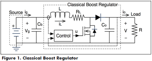
]]> These current harmonics introduce problems for classical sources such as batteries by degrading the source lifetime and generating a sensible problem in portable applications (Kuperman and Aharon, 2011). Similarly, the growth of renewable energy sources has forced the design of high-boosting/low-ripple dc/dc regulators: photovoltaic panels and fuel cells provide low-voltage/high-current dc power, which must be transformed to high-voltage levels to be injected into the grid. In addition, fuel cells are damaged by high current harmonics (Ramos-Paja et al., 2009), while the power generated by photovoltaic panels is strongly reduced in presence of current ripples (Aranda et al., 2009).Consider the classical Boost regulator in Figure 1. Its input current ripple HCR is given by (1), where DCR is the duty cycle and RL models the parasitic losses. From (1), it is noted that high output voltages (high DCR) produce high current ripples.
This problem has been addressed in two ways: first, using large capacitors to filter the current harmonics (Cb in Figure 1) requires electrolytic technology that introduces reliability problems because its high failure rate (Petrone et al. 2008). Second, designing the complex dc/dc converters (Arango et al. 2012) greatly increases the complexity of the circuit analysis and regulation control.

This paper proposes a balanced solution to introduce a self-controlled active pre-filter without affecting the regulator's complexity and control. The solution is based on the parallel connection of the canonical Boost cells, which are controlled with a programmed current control. In addition to its filtering capability, the proposed pre-filter improves the overall efficiency and allows the regulator to provide higher output voltages. Moreover, because electrolytic capacitors are not required, the system reliability is not affected.
Active pre-filter based on parallel converters
The proposed pre-filter is based on the parallel connection of multiple Boost converters. This topology was selected because of its continuous input current and triangular waveform. Then, the converters must be operated to mitigate the current ripple of one converter with the current ripple generated by the other converters, which eventually generates a ripple-free input current. Thus, any power source connected at the pre-filter input will be protected from the current harmonics generated by any load connected at the pre-filter output.
]]> Figure 2 shows the pre-filter structure. The canonical cell is formed by a Boost topology in which the inductor's equivalent series resistance (ESR) collects all the converter losses. This canonical cell is used to construct an N-order filter, where N is the number of cells in parallel. Hence, all the cells have the same input and output voltages and eventually the same duty cycle.
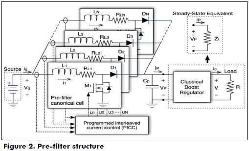
Therefore, the cells' input current (i.e., inductor currents) must be shifted to match the high part of some cells' ripples with the low part of the other cells' ripples. Thus, the cells' ripples are cancelled to produce a ripple-free input current.
In addition, the average currents of all the cells must be the same to avoid overcharging one (or several) cell(s), which could lead to a destructive condition: if a cell is overcharged, its inductor and/or switches (MOSFET and diode) could be damaged; hence, the remaining cells will support an increased current, which could dam- age more cells. To prevent this destructive condition, the pre-filter is regulated to ensure the same average current in all the cells. Figure 2 shows the connection of the programed interleaved current control (PICC) proposed to regulate the pre-filter, which ensures the same current on all the cells. This controller is explained in detail below.
Finally, the pre-filter load could be modeled with a differential resistance Zi that represents the input impedance of the main Boost regulator. In the following sections, the expressions that describe the inductor currents are obtained and used to calculate the optimal shift time for the parallel cells.
Single-cell analysis
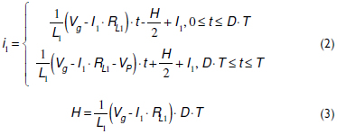
For the system shown in Figure 2, the cell inductor current i1 is given by (2), where I1 represents the average cell current, H represents the amplitude of the current ripple given in (3), D represents the duty cycle, and T represents the switching period.

Then, using the charge and volt-second balances (Erickson and Maksimovic, 2001), the cell voltage conversion ratio M(D)C is given by (5).

Shift time and duty cycle for N = 2
To illustrate the calculation of the shift time and duty cycle required to cancel out the inductor current ripples, the second-order pre-filter (N = 2) is used. Thus, the second cell current i2 is shifted in ΔT seconds, obtaining the expression given in (6), where the average values of both i1 and i2 are the same.
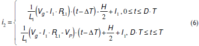
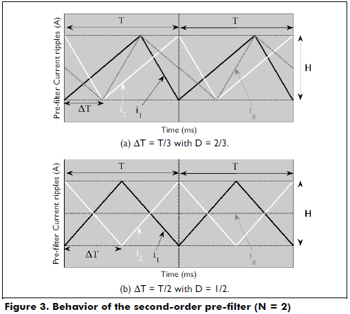
By considering that ig = i1+i2, the mitigation of the current ripple in ig is obtained for i1+i2 = 2I1 = 2I2. Then, replacing (2) and (6) in i1+i2-2I1=0 leads to ΔT = DT. This condition indicates that the high peak of i1 must coincide with the low peak of i2 (and vice-versa) to ensure the ripple's cancelation. Moreover, because there are two cells, each period must exhibit two ΔT time shifts: a first shift ΔT between i1 and i2 and a second shift ΔT between i2 and i1, which leads to:

From (7), it is concluded that the cells must be operated with a duty cycle D = 1/2 with a shift time ΔT = T/2. Figure 3(b) shows this condition, where the input current ig does not exhibit any ripples because of the cancelation between the i1 and i2 ripples.
Shift time and duty cycle for N ≥ 3
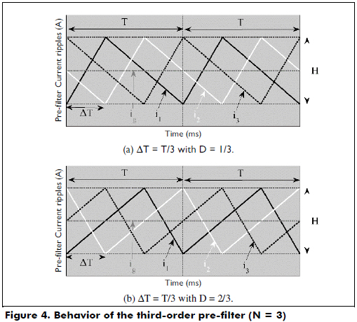
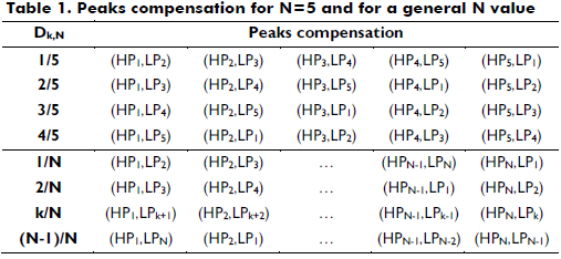
The second-order pre-filter has a single optimal operating condition (ΔT, D), but the high-order (N ≥ 3) pre-filters exhibit more than one optimum. This characteristic is illustrated by using the third-order pre-filter: following the same analyses described for N = 2, the high- and low-ripple peaks of the third-order pre-filter must coincide to provide a ripple-free input current ig. However, to ensure that all the cells exhibit the same switching frequency, the switches of all the cells must be turned on and turned off once in each period. Therefore, because for N = 3 there are three inductor currents, two options are available: the first option considers the high peak of i1 compensated with the low peak of i2 (HP1,LP2), the high peak of i2 compensated with the low peak of i3 (HP2,LP3), and the high peak of i3 compensated with the low peak of i1 (HP3,LP1). The second option considers the compensations given by (HP1,LP3), (HP2,LP1) and (HP3,LP2).
Following the time shifting procedure performed in (6), the waveform of i3 is obtained by shifting i1 in 2ΔT or by shifting i2 in ΔT. Therefore, both operation options for N = 3 require three shift times ΔT in each switching period. Then, following the procedure described for N = 2, the two solutions given in (8) are obtained from i1+i2+i3-3I1=0 to ensure a null ripple in ig. Both solutions require ΔT = T/3.
]]>
Figure 4 shows the behavior of the third-order pre-filter with those solutions: both options provide the desired mitigation between the inductor current ripples to generate a ripple-free ig.
The general expressions for the N-order pre-filter are obtained using the analysis previously described for N = 2 and N = 3. The expressions in (9) describe the optimal operating conditions for any number of cells N, where N-1 solutions could be adopted to mitigate the ripple in ig. In addition, Table 1 presents the peak compensation generated in each optimal duty cycle for N = 5 and for a general N value. This table provides evidence of the multiple operation conditions available for a high-order pre-filter. Therefore, additional criteria are required to select a particular duty cycle among the options given in (9).
Pre-filter voltage conversion ratio
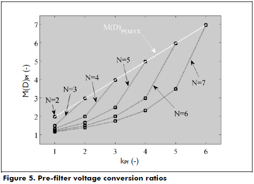
Each optimal duty cycle available for an N-order pre-filter imposes a particular voltage conversion ratio M(D)pf. These voltage conversion ratios are calculated from the single cell M(D)C given in (5) by accounting for the optimal duty cycles given in (9), which leads to the M(D)pf expression given in (10). It is noted that the higher the duty cycle, the higher the voltage conversion ratio. Therefore, the maximum voltage conversion ratio M(D)pf,MAX is achieved for kpf = N-1 as given in (11). This expression considers all of the cells to be equal, i.e., L1 = Lk = L and RL1 = RLk = RL, which is the correct approach to ensure that the cells have the same impedance to simplify the control design.
]]>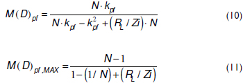
Figure 5 illustrates the M(D)pf for 2 ≤ N ≤ 7, where it is confirmed that M(D)pf,MAX occurs at the maximum kpf = N-1. In addition, it is observed that similar M(D)pf are obtained with different N values, e.g., N = 2, N = 4 with kpf = 2, and N = 6 with kpf = 3. However, higher N values require more complex and costly pre-filters, which suggests that kpf = N-1 must be adopted.
Finally, two characteristics must be noted: first, the correct operation of the pre-filter requires a cell current control; second, the pre-filter allows a classical Boost regulator to significantly increase the regulated voltage conversion ratio. Both characteristics are analyzed in detail in the following sections.
Programmed interleaved current control (PICC)
To ensure uniform current sharing among the cells, the programed interleaved current control (PICC) drives the switches to ensure a maximum difference between the pre-filter inductor currents. This strategy is similar to the hysteretic current control used in classical converters (Erickson and Maksimovic, 2001), but it is extended to several parallel cells.
The PICC detects the conditions for compensating the current ripples given in the last row of Table 1, accounting for the highest voltage conversion ratio. When these conditions appear, the cell's switches are configured to constrain the inductor's current difference. Figure 6 describes the implementation of the PICC for N cells: when the difference between the associated currents (as in Table 1) is higher than the desired limit H, a comparator generates a trigger signal Tk. Then, a rules matrix defines the actions on the switches to avoid an increment in the current difference. For example, if ik+1 - ik ≥ H, i.e., Tk = 1, the control signal uk of the MOSFET k is "Set" to force the increment of ik, while the signal uk+1 of the MOSFET k+1 is "Reset" to force the decrement of ik+1. This action ensures that ik+1 - ik ≤ H, which effectively constrains the cells' current ripple. Finally, the state of the MOSFET control signal is stored in a Set-Reset flip-flop.
]]>
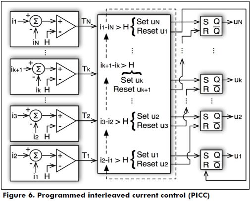
Because the MOSFETs must be switched in the same order given in the last row of Table 1 to guarantee the M(D)pf,MAX, the switching rules Tk must be evaluated sequentially from T1 to TN. Therefore, Tk is considered if Tk-1 was already triggered. This evaluation procedure could be easily implemented in a digital device using a digital hardware description, e.g., VHDL in an FPGA or by using a standard programming language, e.g., C language in a DSP or micro-controller. Finally, the adders, comparators and flip-flops are easily designed with classical analog components.
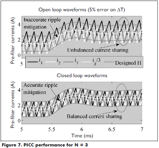
Figure 7 shows the operation of a third-order pre-filter with the following cell parameters: L1 = Lk = L = 1 mH, RL1 = RLk = RL = 50 mW, CP = 6.8 mF and Zi = 50 W. The simulation also considers Vg = 24 V, H = 0.8 A and a load perturbation at t = 5.4 ms to Zi = 25 W. The upper traces of Figure 7 consider an open loop operation with a constant duty cycle (11) and a fixed shift time ΔT because the element tolerances and aging exhibit an error of 5 %. The simulation results show that this small error generates significant differences in the average currents, which deteriorates the ripple mitigation and overcharges a cell. Instead, the bottom traces of Figure 7 consider the action of the PICC, where the cell ripples are constrained to the desired H magnitude, ensuring balanced current sharing among the cells and providing a satisfactory ripple-free input current. A similar condition is obtained for small differences in the cells' parameters: in a closed loop, the cells' ripples are constrained, while in an open loop, several differences appear.
Pre-filter-based regulators
As previously described, the pre-filter filters the current harmonics generated by classical regulators, and at the same time, it improves the Boost regulator characteristics. The pre-filter is connected in series with the Boost regulator as shown in Figure 2. Therefore, the load impedance interacting with the pre-filter is the input impedance of the Boost regulator.
Moreover, the voltage conversion ratio and efficiency of this series connected regulator, called the pre-filter-based regulator, depend on both the pre-filter and the regulator. Therefore, the following subsections review the classical Boost regulator characteristics to analyze the pre-filter-based regulator.
Classical Boost Regulator characteristics
The classical boost regulator (CR) depicted in Figure 1 transforms the source power to the supply regulated power to the load R. To provide a fair comparison, the CR is considered along with the same elements adopted for the pre-filter. In practice, this is the worst case because smaller inductors could be used for the pre-filter, exhibiting lower losses and improving the efficiency.
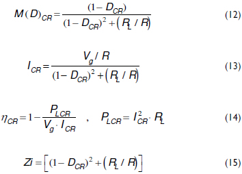
]]> The CR voltage conversion ratio is given in (12), while the average inductor current is given in (13) (Erickson and Maksimovic, 2001). Similarly, considering the power losses PLCR that occur in RL, the CR efficiency is given in (14). Finally, the CR input impedance, i.e., the pre-filter load, is given in (15).
Pre-filter-based regulator characteristics
From the pre-filter-based (Pf-R) scheme of Figure 2, the following electrical characteristics hold: the cells exhibit an average current I1 = I2 = IK = IS, where IS represents the average current of the CR inductor generated by its interaction with the pre-filter and the load. This condition is deduced from the average current of the pre-filter diodes, ID = IS/N, which leads to the average inductor currents Ik = ID/(Dk,N)=N×ID=IS.
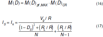
The Pf-R voltage conversion ratio M(D) is given in (16), where Zi in (11) is given by (15). Similarly, from (11) and (13), the inductor average currents (cells and CR) are given by (17), where DS represents the CR duty cycle required in the Pf-R solution.
Then, the efficiency and power losses on the Pf-R circuit are given in (18). To contrast the power losses on both CR and Pf-R circuits, the improvement losses ratio βpf-R/CR is defined in (19). Because βpf-R/CR < 1 for N ≥ 2, it is evident that the pre-filter-based regulator has a higher efficiency in comparison with the classical Boost regulator.
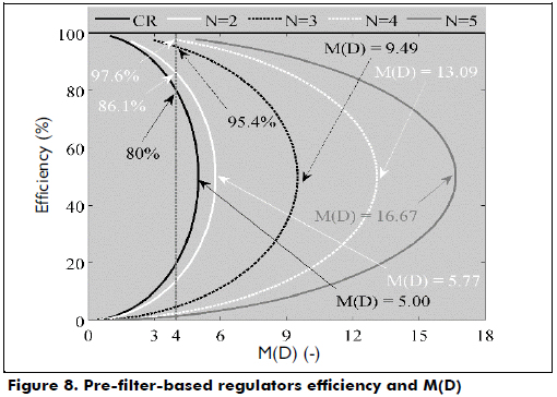
Figure 8 shows the simulation of both Pf-R and CR circuits for different M(D) conditions. The simulations consider the same parameters described in the previous section. The results show that the Pf-R solution can provide the same M(D) as the CR solution but with an improved efficiency, e.g., for M(D) = 4, the Pf-R with N = 2 improves by 6.1 % of the regulator efficiency, while the Pf-R with N = 3 improves the efficiency by 15.4 %. Moreover, the Pf-R solution allows higher voltage conversion ratios that are not achievable by CR alone, e.g., with N = 3, the Pf-R provides M(D) = 6 with an efficiency equal to 90 %, and the Pf-R with N = 5 provides a maximum M(D) = 16.7, while the maximum M(D) for the CR is 5.0. These results provide evidence of the significant improvement in the efficiency and voltage conversion ratio generated for the classical Boost regulator by the pre-filter operation.
]]>
Experimental results
To experimentally validate the proposed solution, the proof-of-concept prototype depicted in Figure 9 was developed. This prototype consists of a second-order pre-filter interacting with a classical Boost regulator. The prototype is controlled with a Virtex-5 FPGA that is programmed using a JTAG device. Moreover, the comparators and adders were implemented with analog circuitry.
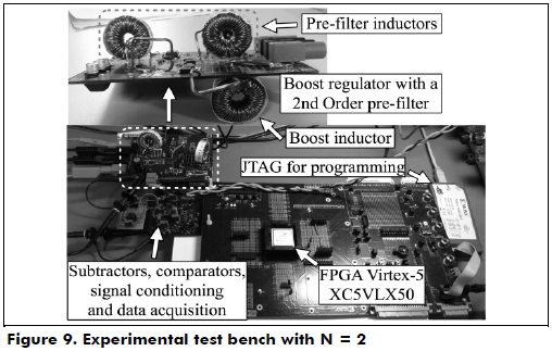
Figure 10 shows the pre-filter-based waveforms at both high (top) and low (bottom) load current conditions: because the Boost regulator operates in a continuous conduction mode (CCM in top) or in a discontinuous conduction mode (DCM in bottom), the pre-filter cell currents are accurately shifted to provide a ripple-free input current. Moreover, because the tolerances of the cells' elements generate some differences among the cells' impedances, the input current does not exhibit a significant ripple because of the correctness of the proposed controller.
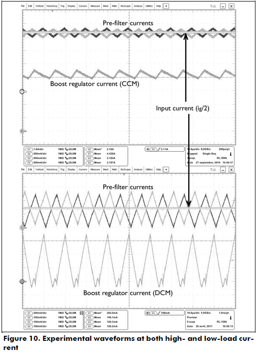
Figure 11 shows the experimental efficiency hpf-R of the pre-filter-based regulator for different M(D) conditions. In addition, the figure presents the experimental losses ratio bpf-R/CR, where the efficiency improvement provided by the pre-filter to the classical Boost regulator is observed. Similarly, the M(D) conditions that are not achievable with the CR prototype but are achievable with the Pf-R prototype are also highlighted.
]]>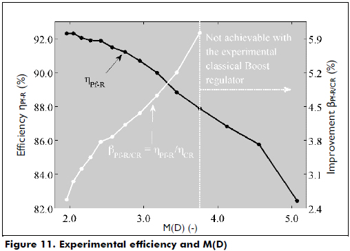
Finally, these experimental results validate the analytical and simulation results presented previously. The experiments illustrate the benefits of introducing the proposed pre-filter structure between the source and the regulator: current harmonics filtering, improved efficiency and higher voltage conversion ratio.
Conclusions
An active pre-filter was proposed to protect the source from the regulators' current ripples. The pre-filter also increases the overall efficiency and achieves higher voltage conversion ratios. Moreover, the pre-filter provides the same voltage conversion ratio as the classical solutions but with an improved efficiency. In addition, the pre-filter does not affect the main regulator control. Similarly, the pre-filter's main drawback consists in an increased number of elements, which increases the solution size and cost. Furthermore, modern drivers with diode-MOSFET synchronization or even synchronous boost topologies are desirable to avoid the commutation problems among the pre-filter branches in practical implementations.
Finally, the proposed solution is a suitable option for improving the characteristics of the classical Boost regulators dedicated to low-ripple/high-boosting applications, such as photovoltaic and fuel cell power systems.
Acknowledgments
This work was supported by the Universidad Nacional de Colombia under the project RECONF-PV-18789, the Universitat Rovira i Vitgili, and the R&D division of TOTAL.EN.
References
Aranda, E. D., Galan, J. A. G., de Cardona, M. S., & Marquez, J. M. A. (2009). Measuring the I-V curve of PV generators. IEEE Industrial Electronics Magazine, 3(3), 4-14. [ Links ]
Arango, E., Ramos-Paja, C. A., Calvente, J., Giral, R., & Serna, S. (2012). Asymmetrical Interleaved DC/DC Switching Converters for Photovoltaic and Fuel Cell Applications-Part 1: Circuit Generation, Analysis and Design. Energies, 5, 4590-4623. [ Links ]
Erickson, R. W., & Maksimovic, D. (2001). Fundamentals of Power Electronics (2nd ed.). New York, NY: Springer. [ Links ]
Kuperman, A., & Aharon, I. (2011). Battery-ultracapacitor hybrids for pulsed current loads: A review. Renewable and Sustainable Energy Reviews, 15(2), 981-992. [ Links ]
Petrone, G., Spagnuolo, G., Teodorescu, R., Veerachary, M., & Vitelli, M. (2008). Reliability Issues in Photovoltaic Power Processing Systems. IEEE Transactions on Industrial Electronics, 55(7), 2569-2580. [ Links ]
Ramos-Paja, C. A., Bordons, C., Romero, A., Giral, R., & Martinez-Salamero, L. (2009). Minimum Fuel Consumption Strategy for PEM Fuel Cells. IEEE Transactions on Industrial Electronics, 56(3), 685-696. [ Links ]
Taghvaee, M.H., Radzi, M.A.M., Moosavain, S.M., Hizam, H., & Marhaban, M. (2013). A current and future study on non-isolated DC-DC converters for photovoltaic applications. Renewable and Sustainable Energy Reviews, 17, 216-227. [ Links ]
Veerachary, M., Senjyu, T., & Uezato, K. (2003). Modeling of closed-loop voltage-mode controlled interleaved dual boost converter. Computers & Electrical Engineering, 29(1), 67-84. [ Links ]
]]>