<?xml version="1.0" encoding="ISO-8859-1"?><article xmlns:mml="http://www.w3.org/1998/Math/MathML" xmlns:xlink="http://www.w3.org/1999/xlink" xmlns:xsi="http://www.w3.org/2001/XMLSchema-instance">
<front>
<journal-meta>
<journal-id>0120-6230</journal-id>
<journal-title><![CDATA[Revista Facultad de Ingeniería Universidad de Antioquia]]></journal-title>
<abbrev-journal-title><![CDATA[Rev.fac.ing.univ. Antioquia]]></abbrev-journal-title>
<issn>0120-6230</issn>
<publisher>
<publisher-name><![CDATA[Facultad de Ingeniería, Universidad de Antioquia]]></publisher-name>
</publisher>
</journal-meta>
<article-meta>
<article-id>S0120-62302010000200014</article-id>
<title-group>
<article-title xml:lang="en"><![CDATA[Parallelogram Based Method for Space Vector Pulse Width Modulation]]></article-title>
<article-title xml:lang="es"><![CDATA[Modulación por Ancho de Pulso de Vectores Espaciales utilizando el Método del Paralelogramo]]></article-title>
</title-group>
<contrib-group>
<contrib contrib-type="author">
<name>
<surname><![CDATA[Restrepo]]></surname>
<given-names><![CDATA[José]]></given-names>
</name>
<xref ref-type="aff" rid="A01"/>
</contrib>
<contrib contrib-type="author">
<name>
<surname><![CDATA[Guzmán]]></surname>
<given-names><![CDATA[Víctor]]></given-names>
</name>
<xref ref-type="aff" rid="A01"/>
</contrib>
<contrib contrib-type="author">
<name>
<surname><![CDATA[Giménez]]></surname>
<given-names><![CDATA[María]]></given-names>
</name>
<xref ref-type="aff" rid="A01"/>
</contrib>
<contrib contrib-type="author">
<name>
<surname><![CDATA[Bueno]]></surname>
<given-names><![CDATA[Alexander]]></given-names>
</name>
<xref ref-type="aff" rid="A01"/>
</contrib>
<contrib contrib-type="author">
<name>
<surname><![CDATA[Aller]]></surname>
<given-names><![CDATA[José]]></given-names>
</name>
<xref ref-type="aff" rid="A01"/>
</contrib>
</contrib-group>
<aff id="A01">
<institution><![CDATA[,Universidad Simón Bolívar Grupo de Sistemas Industriales de Electrónica de Potencia ]]></institution>
<addr-line><![CDATA[Caracas ]]></addr-line>
<country>Venezuela</country>
</aff>
<pub-date pub-type="pub">
<day>00</day>
<month>03</month>
<year>2010</year>
</pub-date>
<pub-date pub-type="epub">
<day>00</day>
<month>03</month>
<year>2010</year>
</pub-date>
<numero>52</numero>
<fpage>161</fpage>
<lpage>171</lpage>
<copyright-statement/>
<copyright-year/>
<self-uri xlink:href="http://www.scielo.org.co/scielo.php?script=sci_arttext&amp;pid=S0120-62302010000200014&amp;lng=en&amp;nrm=iso"></self-uri><self-uri xlink:href="http://www.scielo.org.co/scielo.php?script=sci_abstract&amp;pid=S0120-62302010000200014&amp;lng=en&amp;nrm=iso"></self-uri><self-uri xlink:href="http://www.scielo.org.co/scielo.php?script=sci_pdf&amp;pid=S0120-62302010000200014&amp;lng=en&amp;nrm=iso"></self-uri><abstract abstract-type="short" xml:lang="en"><p><![CDATA[This paper presents a parallelogram based duty cycle computation method for space vector modulation control using standard pulse width modulation circuitry. This technique maps the voltage source inverter&rsquo;s solution space into only three parallelogram shaped zones and reduces the computational load. The proposed modulation methods are especially suited for a description of the voltage space vector in its &alpha;, &beta; components and for modern and high dynamic applications, where demand changes may happen at a frequency comparable with the modulator carrier frequency. Several modulation methods used in scalar applications and extensively studied in the literature are easily obtained by combining the use of the modulation methods proposed in this work. The proposed methods have been validated by simulations and experimental test.]]></p></abstract>
<abstract abstract-type="short" xml:lang="es"><p><![CDATA[Este artículo presenta un método para la determinación del ciclo de trabajo de la modulación de vectores espaciales utilizando circuitos convencionales de modulación por ancho de pulso. Este método utiliza tres paralelogramos que cubren el espacio hexagonal de la salida del inversor, reduciendo de esta forma el esfuerzo de cálculo computacional. La metodología propuesta es aplicable directamente a la descripción de las componentes &alpha;, &beta; del vector espacial en controladores modernos, con altos requerimientos dinámicos, donde la demanda de cambios se realiza a una frecuencia comparable con la de la señal portadora. Combinando las estrategias de modulación DPWMMIN y DPWMMAX propuestas en este trabajo, se obtiene fácilmente el ciclo de trabajo para otros métodos de modulación, utilizados en aplicaciones escalares y ampliamente estudiadas en la literatura. El método propuesto ha sido comprobado mediante simulaciones y ensayos experimentales.]]></p></abstract>
<kwd-group>
<kwd lng="en"><![CDATA[Index Terms]]></kwd>
<kwd lng="en"><![CDATA[PWM]]></kwd>
<kwd lng="en"><![CDATA[inverters]]></kwd>
<kwd lng="en"><![CDATA[DC-AC power conversion]]></kwd>
<kwd lng="en"><![CDATA[space vector]]></kwd>
<kwd lng="en"><![CDATA[space vector modulation]]></kwd>
<kwd lng="en"><![CDATA[parallelogram]]></kwd>
<kwd lng="es"><![CDATA[PWM]]></kwd>
<kwd lng="es"><![CDATA[inversores]]></kwd>
<kwd lng="es"><![CDATA[conversión de potencia CC-CA]]></kwd>
<kwd lng="es"><![CDATA[vectores espaciales]]></kwd>
<kwd lng="es"><![CDATA[modulación de vectores espaciales, paralelogramo]]></kwd>
</kwd-group>
</article-meta>
</front><body><![CDATA[ <p align="center"><font face="Verdana" size="4"> <b>Parallelogram Based Method for Space Vector Pulse Width Modulation</b></font></p>     <p align="center"><font face="Verdana" size="4"> <b>Modulaci&oacute;n por Ancho de Pulso de Vectores Espaciales utilizando el M&eacute;todo del Paralelogramo</b></font></p>     <p> <font face="Verdana" size="2"> <i>Jos&eacute; Restrepo<sup>*</sup>, V&iacute;ctor Guzm&aacute;n, Mar&iacute;a Gim&eacute;nez, Alexander Bueno, Jos&eacute; Aller</i></font></p>     <p><font face="Verdana" size="2">Universidad Sim&oacute;n Bol&iacute;var, Grupo de Sistemas Industriales de Electr&oacute;nica de Potencia Caracas 1080A &#45; Venezuela</font></p>     <p><font face="Verdana" size="2">&nbsp;</font></p> <hr noshade size="1">      <p><font face="Verdana" size="3"><b>Abstract</b></font></p>     <p><font face="Verdana" size="2">This paper presents a parallelogram based duty cycle computation method for space vector modulation control using standard pulse width modulation circuitry. This technique maps the voltage source inverter&rsquo;s solution space into only three parallelogram shaped zones and reduces the computational load. The proposed modulation methods are especially suited for a description of the voltage space vector in its &alpha;, &beta; components and for modern and high dynamic applications, where demand changes may happen at a frequency comparable with the modulator carrier frequency. Several modulation methods used in scalar applications and extensively studied in the literature are easily obtained by combining the use of the modulation methods proposed in this work. The proposed methods have been validated by simulations and experimental test.</font></p>     <p><font face="Verdana" size="2"><b>Keywords:</b> Index Terms, PWM, inverters, DC&#45;AC power conversion, space vector, space vector modulation, parallelogram.</font></p>     <p><font face="Verdana" size="2">&nbsp;</font></p> <hr noshade size="1">     <p><font face="Verdana" size="3"><b>Resumen</b></font></p>     ]]></body>
<body><![CDATA[<p><font face="Verdana" size="2">Este art&iacute;culo presenta un m&eacute;todo para la determinaci&oacute;n del ciclo de trabajo de la modulaci&oacute;n de vectores espaciales utilizando circuitos convencionales de modulaci&oacute;n por ancho de pulso. Este m&eacute;todo utiliza tres paralelogramos que cubren el espacio hexagonal de la salida del inversor, reduciendo de esta forma el esfuerzo de c&aacute;lculo computacional. La metodolog&iacute;a propuesta es aplicable directamente a la descripci&oacute;n de las componentes &alpha;, &beta; del vector espacial en controladores modernos, con altos requerimientos din&aacute;micos, donde la demanda de cambios se realiza a una frecuencia comparable con la de la se&ntilde;al portadora. Combinando las estrategias de modulaci&oacute;n DPWMMIN y DPWMMAX propuestas en este trabajo, se obtiene f&aacute;cilmente el ciclo de trabajo para otros m&eacute;todos de modulaci&oacute;n, utilizados en aplicaciones escalares y ampliamente estudiadas en la literatura. El m&eacute;todo propuesto ha sido comprobado mediante simulaciones y ensayos experimentales.</font></p>     <p><font face="Verdana" size="2"><b>Palabras clave:</b> PWM, inversores, conversi&oacute;n de potencia CC&#45;CA, vectores espaciales, modulaci&oacute;n de vectores espaciales, paralelogramo</font></p>     <p><font face="Verdana" size="2">&nbsp;</font></p> <hr noshade size="1">     <p><font face="Verdana" size="3"><b>Introduction</b></font></p>     <p><font face="Verdana" size="2">The standard voltage source inverter &#40;VSI&#41;, shown in figure 1a, can be found in many modern applications requiring precise control of power flow from AC to DC or vice versa, and much research has been devoted towards the development of efficient ways for controlling this type of converters [1&#45;6]. From the many techniques used in the control of power converters, Pulse Width Modulation &#40;PWM&#41; has been in general the preferred choice, and over the past decades several variants of this technique have been studied. With the availability of new logic circuits of constantly increasing processing power, high performance control strategies based on space vector theory are possible, and Space Vector Pulse Width Modulation &#40;SVPWM&#41; seems especially suited for these and similar high dynamic control schemes. Although SVPWM has also been a subject of extensive research [7&#45;22], there are few algorithms using the description of average voltages in natural &#40;a, b, c&#41; coordinates [19], an even less employing the description in &#40;&alpha;, &beta;&#41; coordinates. In general, most of the published works deal with waveforms in quasisteady state &#40;per modulating period dynamics&#41;, where space vector advantages are not fully explored. In this work, an algorithm specially suited for applications requiring the generation of a per carrier period average voltage space vector in the &#40;&alpha;, &beta;&#41; plane is proposed. This algorithm maps the inverter output voltage space state into three parallelogram sectors, as shown in<a href="#Figura1"> figure 1b</a>, covering the hexagonal shape of the locus of possible per carrier period average space vectors produced by the converter shown in <a href="#Figura1">figure 1&#40;a&#41;</a>. The proposed algorithm main advantage is a significant reduction in execution time during the computation of duty cycle demands for the PWM circuitry. For this, the duty cycle for each converter branch is obtained with a reduced number of arithmetic and logic operations and without using complex mathematical functions such as square roots, or trigonometric functions. The demanded average space vector <img src="/img/revistas/rfiua/n52/n52a14i01.gif" ><sub>s</sub> is synthesized using the triangle intersection technique, as in most PWM circuits. Seven modern modulation techniques are analyzed combining the use of Discontinuous Pulse Width Modulation Minimum and Maximum &#40;DPWMMIN, DPWMMAX&#41;. The performance of the modulation methods is verified with experimental tests, and the results are presented in this paper.</font></p>      <p><font face="Verdana" size="3"><b>Methodology</b></font></p>     <p><font face="Verdana" size="2"><b>Space vector modulation</b></font></p>     <p><font face="Verdana" size="2">The typical three&#45;phase converter shown in figure 1&#40;a&#41; has 4<sup>3</sup> &#61; 64 possible states; of which  only the 2<sup>3</sup> &#61; 8 states having a single power device turned “on” in each branch can be used in practice. Three of these states can be considered as a base to produce the remaining five states. Figure 1&#40;b&#41; shows the three base vectors <img src="/img/revistas/rfiua/n52/n52a14i01.gif" ><sub>a</sub>,  <img src="/img/revistas/rfiua/n52/n52a14i01.gif" ><sub>b</sub> and  <img src="/img/revistas/rfiua/n52/n52a14i01.gif" ><sub>c</sub>, corresponding to states &#40;1,0,0&#41;, &#40;0,1,0&#41; and &#40;0,0,1&#41; respectively, and the hexagon vertices are identified by a number representing the bridge connectivity. In this representation a “1”  corresponds to an upper power device turned “on” while the lower device is turned “off”, and a “0” corresponds to a lower power device turned “on” while the upper device is turned “off”.</font></p>     <p align="center"><font face="Verdana" size="2"><img src="/img/revistas/rfiua/n52/n52a14i02.gif" ><a name="Figura1"></a></font></p>       <p><font face="Verdana" size="2"><b>Figure 1</b> Voltage source inverter &#40;VSI&#41; circuit diagram and output voltage space</font></p>     ]]></body>
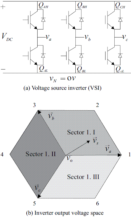
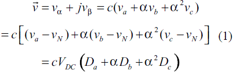
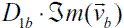
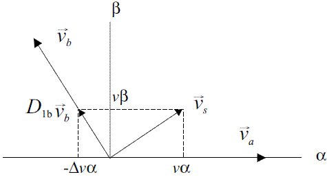
<body><![CDATA[<p><font face="Verdana" size="2">Any average voltage space vector inside the hexagonal shape shown in figure 1&#40;b&#41; can be obtained by using the Clarke transformation:</font></p>     <p><font face="Verdana" size="2"><img src="/img/revistas/rfiua/n52/n52a14i03.gif" ><a name="Ecuaci&oacute;n1"></a></font></p>      <p><font face="Verdana" size="2">Where <img src="/img/revistas/rfiua/n52/n52a14i04.gif" >, and <i>D<sub>a</sub>, D<sub>b</sub>, D<sub>c</sub></i>, are the duty cycles for each inverter branch; c usually takes the values 1, 2&#47;3 or <img src="/img/revistas/rfiua/n52/n52a14i05.gif" >.</font></p>      <p><font face="Verdana" size="2">In the three phase coordinates, the three base vectors are &alpha;<sub>1</sub>, &alpha;<sub>2</sub> and &alpha;<sub>3</sub>, of unitary magnitude; each phase generates a spatial vector in the corresponding direction, whose magnitude is found to be <img src="/img/revistas/rfiua/n52/n52a14i06.gif" > &#40;<i>c</i> is a scale factor set by the mathematical transformation used in the vector calculation&#41;, and with Pulse Width Modulation during a carrier signals period, each branch average voltage can be modified. Since the zero vector can be synthesized using states <i><i>&#40;0,0,0&#41;</i></i> or <i>&#40;1,1,1&#41;</i>, there are in theory infinite possible combinations to synthesize an average voltage space vector using standard triangular carrier modulators. As a consequence of this large amount of possible combinations for synthesizing voltage space vectors, SVPWM can be found in the literature under different names [12, 13, 23]. To simplify the analysis, in this work three possible methods are used to synthesize any space vector in the hexagonal locus covered by the base vectors using carrier based modulation, usually known as Discontinuous Pulse Width Modulation Minimum &#40;DPWMMIN&#41;, Discontinuous Pulse Width Modulation Maximum &#40;DPWMMAX&#41; and SVPWM in the literature [12]. However, there are other switching strategies, such as sequences type III and type IV [21], or special sequences for ripple minimization that are not suitable for standard triangular carrier implementations [18, 21, 24].</font></p>      <p><font face="Verdana" size="2"><b>Discontinuous PWM minimum &#40;DPWMMIN&#41;</b></font></p>     <p><font face="Verdana" size="2">In DPWMMIN [12, 23], the desired average voltage space vector <img src="/img/revistas/rfiua/n52/n52a14i01.gif" > <sub>s</sub> &#61; <i>v</i><sub>&alpha;</sub> + <i>jv<sub>&beta;</sub></i> is synthesized by adjusting the two neighboring base vectors magnitude with PWM and at the same time setting the remaining base vector to zero; in this case the zero vector is produced with state <i><i>&#40;0,0,0&#41;</i></i>. <a href="#Figura1">Figure 1&#40;b&#41;</a> shows the three parallelograms defining three different sectors used in the synthesis of any average voltage space vector <img src="/img/revistas/rfiua/n52/n52a14i01.gif" ><sub>s</sub> in the hexagonal space vector locus. <a href="#Figura2">Figure 2</a> shows the decomposition of a space vector <img src="/img/revistas/rfiua/n52/n52a14i01.gif" ><sub>s</sub> in sector 1.I. In this case <img src="/img/revistas/rfiua/n52/n52a14i07.gif" >   &#40;produces the &beta; component of <img src="/img/revistas/rfiua/n52/n52a14i01.gif" ><sub>s</sub> and <img src="/img/revistas/rfiua/n52/n52a14i08.gif" > produces the vector component <img src="/img/revistas/rfiua/n52/n52a14i09.gif" > that needs to be compensated with part of base vector <img src="/img/revistas/rfiua/n52/n52a14i01.gif" ><sub>a</sub>.</font></p>      <p align="center"><font face="Verdana" size="2"><img src="/img/revistas/rfiua/n52/n52a14i10.gif" ><a name="Figura2"></a></font></p>      <p><font face="Verdana" size="2"><b>Figure 2</b> Decomposition <img src="/img/revistas/rfiua/n52/n52a14i01.gif" ><sub>s</sub> of in sector 1.I using the DPWMMIN modulation system</font></p>      <p><font face="Verdana" size="2">By using the following auxiliary variables:</font></p>     <p><font face="Verdana" size="2"><img src="/img/revistas/rfiua/n52/n52a14i11.gif" ><a name="Ecuaci&oacute;n2"></a></font></p>       ]]></body>
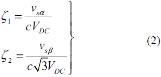
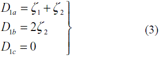
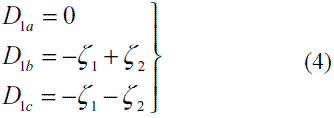
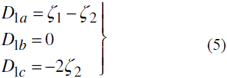
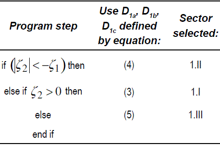
<body><![CDATA[<p><font face="Verdana" size="2">The equations defining the duty cycles required to synthesize any average voltage space vector using DPWMMIN as a function of the parallelogram sectors shown in <a href="#Figura1">figure 1&#40;b&#41;</a>, are:</font></p>     <p><font face="Verdana" size="2">1&#41; Sector 1.I:</font></p>      <p><font face="Verdana" size="2"><img src="/img/revistas/rfiua/n52/n52a14i12.gif" ><a name="Ecuaci&oacute;n3"></a></font></p>      <p><font face="Verdana" size="2">2&#41; Sector 1.II:</font></p>      <p><font face="Verdana" size="2"><img src="/img/revistas/rfiua/n52/n52a14i13.gif" ><a name="Ecuaci&oacute;n4"></a></font></p>      <p><font face="Verdana" size="2">3&#41; Sector 1.III:</font></p>     <p><font face="Verdana" size="2"><img src="/img/revistas/rfiua/n52/n52a14i14.gif" ><a name="Ecuaci&oacute;n5"></a></font></p>      <p><font face="Verdana" size="2">The sector selection algorithm for DPWMMIN is presented in Table 1.</font></p>     <p><font face="Verdana" size="2"><b>Table 1</b> Sector selection algorithm for DPWMMIN modulation using the proposed method.</font></p>     <p align="center"><font face="Verdana" size="2"><img src="/img/revistas/rfiua/n52/n52a14i15.gif" ><a name="Tabla1"></a></font></p>      ]]></body>
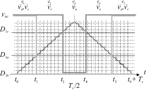
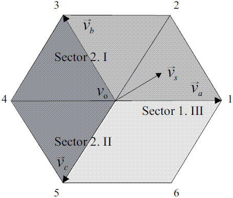
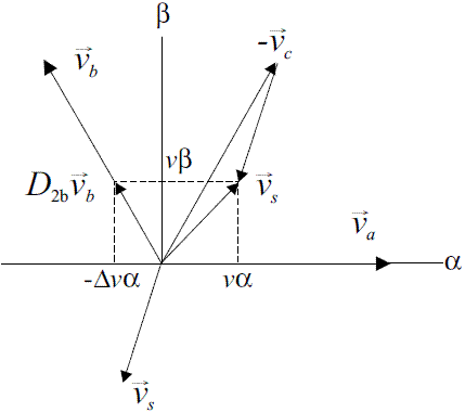
<body><![CDATA[<p><font face="Verdana" size="2"><a href="#Figura3">Figure 3</a> shows an example of the control signals that must be applied to the power devices in each branch when a PWM with central symmetry is used to synthesize a space vector with this modulating strategy. In this example the average voltage space vector reference is in sector 1.III and the resulting instantaneous VSI vector sequence is <img src="/img/revistas/rfiua/n52/n52a14i16.gif" > for <i>D<sub>1c</sub> &gt; D<sub>1a</sub></i>; the null vector <img src="/img/revistas/rfiua/n52/n52a14i01.gif" ><sub>0</sub> is synthesized with state <i>&#40;0,0,0&#41;</i>.</font></p>      <p align="center"><font face="Verdana" size="2"><img src="/img/revistas/rfiua/n52/n52a14i17.gif" ><a name="Figura3"></a></font></p>     <p><font face="Verdana" size="2"><b>Figure 3</b> Firing sequence for a PWM with central symmetry, DPWMMIN modulation method</font></p>      <p><font face="Verdana" size="2"><b>Discontinuous PWM maximum &#40;DPWMMAX&#41;</b></font></p>     <p><font face="Verdana" size="2">In DPWMMAX [12, 23], the base space vector closer to the space vector to be synthesized is turned “on”, and the magnitude of the remaining two base space vectors is adjusted with PWM; in this case zero vector <i>v<sub>0</sub></i> is produced with state <i>&#40;1,1,1&#41;</i> [13].</font></p>      <p><font face="Verdana" size="2"><a href="#Figura4">Figure 4</a> shows the three parallelograms defining three different sectors used in DPWMMAX to synthesize any average voltage space vector <img src="/img/revistas/rfiua/n52/n52a14i01.gif" ><sub>s</sub>, and <a href="#Figura5">figure 5</a> shows the decomposition of a space vector <img src="/img/revistas/rfiua/n52/n52a14i01.gif" ><sub>s</sub>  in sector 2.II. In this case the effect of turning “on” branch c during the whole switching period is that phases a and b have to synthesize space vector <img src="/img/revistas/rfiua/n52/n52a14i01.gif" ><sub>s</sub>, obtained with the following expression:</font></p>      <p><font face="Verdana" size="2"><img src="/img/revistas/rfiua/n52/n52a14i18.gif" ><a name="Ecuaci&oacute;n6"></a></font></p>      <p align="center"><font face="Verdana" size="2"><img src="/img/revistas/rfiua/n52/n52a14i19.gif" ><a name="Figura4"></a></font></p>     <p><font face="Verdana" size="2"><b>Figure 4</b> Base space vectors and parallelogram sectors for DPWMMAX</font></p>      <p><font face="Verdana" size="2">In general, the equations defining the duty cycles required to synthesize any vector using DPWMMAX as a function of the sectors shown in <a href="#Figura4">figure 4</a> are:</font></p>     ]]></body>
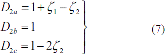
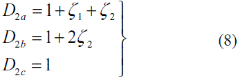
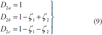
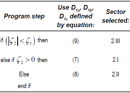
<body><![CDATA[<p><font face="Verdana" size="2">1&#41; Sector 2.I:</font></p>     <p><font face="Verdana" size="2"><img src="/img/revistas/rfiua/n52/n52a14i20.gif" ><a name="Ecuaci&oacute;n7"></a></font></p>     <p><font face="Verdana" size="2">2&#41; Sector 2.II:</font></p>      <p><font face="Verdana" size="2"><img src="/img/revistas/rfiua/n52/n52a14i21.gif" ><a name="Ecuaci&oacute;n8"></a></font></p>     <p><font face="Verdana" size="2">3&#41; Sector 2.III:</font></p>     <p><font face="Verdana" size="2"><img src="/img/revistas/rfiua/n52/n52a14i22.gif" ><a name="Ecuaci&oacute;n9"></a></font></p>      <p><font face="Verdana" size="2">The sector selection algorithm for DPWMMAX is presented in <a href="#Tabla2">table 2</a>.</font></p>       <p align="center"><font face="Verdana" size="2"><img src="/img/revistas/rfiua/n52/n52a14i23.gif" ><a name="Figura5"></a></font></p>     <p><font face="Verdana" size="2"><b>Figure 5</b> Decomposition of <img src="/img/revistas/rfiua/n52/n52a14i01.gif" ><sub>s</sub> in sector 2.II using the DPWMMAX modulation system</font></p>      <p><font face="Verdana" size="2"><b>Table 2</b> Sector selection algorithm for DPWMMAX modulation using the proposed method</font></p>       ]]></body>
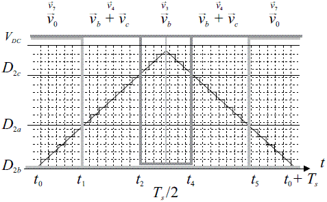
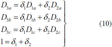
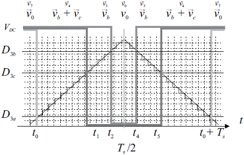
<body><![CDATA[<p><font face="Verdana" size="2"><img src="/img/revistas/rfiua/n52/n52a14i24.gif" ><a name="Tabla2"></a></font></p>     <p><font face="Verdana" size="2"><a href="#Figura6">Figure 6</a> shows an example of the control signals that must be applied to the power devices in each branch when a PWM with central symmetry is used to synthesize a space vector with this modulating strategy. In this example the vector to synthesize is in sector 2.I and the resulting instantaneous VSI vector sequence is <img src="/img/revistas/rfiua/n52/n52a14i25.gif" > for <i>D<sub>2c</sub> &gt; D<sub>2a</sub></i>; the null vector <img src="/img/revistas/rfiua/n52/n52a14i01.gif" ><sub>0</sub> is synthesized with state <i>&#40;1,1,1&#41;</i>.</font></p>       <p align="center"><font face="Verdana" size="2"><img src="/img/revistas/rfiua/n52/n52a14i26.gif" ><a name="Figura6"></a></font></p>     <p><font face="Verdana" size="2"><b>Figure 6</b> Firing sequence for a PWM with central symmetry, DPWMMAX method</font></p>     <p><font face="Verdana" size="2"><b>Space Vector Pulse Width Modulation &#40;SVPWM&#41;</b></font></p>     <p><font face="Verdana" size="2">In SVPWM [12, 23] the duty cycle defining the conduction of the power devices in each branch is obtained by averaging the duty cycle obtained using DPWMMIN and DPWMMAX. In this way, zero vector <i>v<sub>0</sub></i> is synthesized with both states <i>&#40;0,0,0&#41;</i> and &#40;1,1,1&#41; [13]; in a more general form, the duty cycle is computed using the following equations.</font></p>      <p><font face="Verdana" size="2"><img src="/img/revistas/rfiua/n52/n52a14i27.gif" ><a name="Ecuaci&oacute;n10"></a></font></p>      <p><font face="Verdana" size="2"><a href="#Figura7">Figure 7</a> shows an example of the control signals that must be applied to the power devices in each branch when a PWM with central symmetry is used to synthesize a space vector with this modulating strategy. In this example the space vector is synthesized with base vectors <img src="/img/revistas/rfiua/n52/n52a14i01.gif" ><sub>b</sub> and <img src="/img/revistas/rfiua/n52/n52a14i01.gif" ><sub>c</sub>, and the resulting instantaneous VSI vector sequence is <img src="/img/revistas/rfiua/n52/n52a14i28.gif" > for <i>D<sub>3b</sub> &gt; D<sub>3c</sub> &gt; D<sub>3a</sub></i>. The relative size of constants &delta;<sub>1</sub> and &delta;<sub>2</sub> used to synthesize v0 define the relative duration in time of states <i>&#40;0,0,0&#41;</i> and <i>&#40;1,1,1&#41;</i>. Figure 7 shows the case when &delta;<sub>1</sub> &#61; &delta;<sub>2</sub> &#61; 0.5.</font></p>         <p align="center"><font face="Verdana" size="2"><img src="/img/revistas/rfiua/n52/n52a14i29.gif" ><a name="Figura7"></a></font></p>     <p><font face="Verdana" size="2"><b>Figure 7</b> Firing sequence for a PWM with central symmetry, SVPWM method</font></p>      ]]></body>
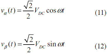
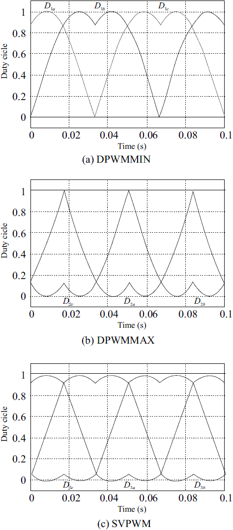
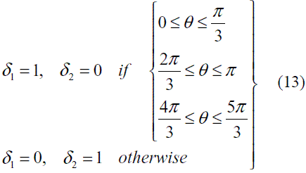
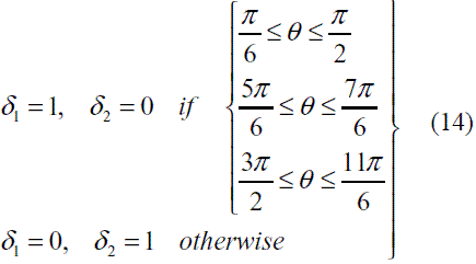
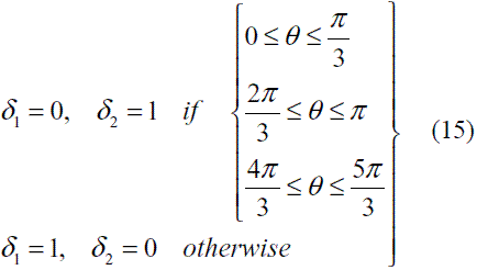
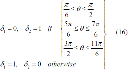
<body><![CDATA[<p><font face="Verdana" size="2"><a href="#Figura8">Figures 8&#40;a&#41; to 8&#40;c&#41;</a> show the typical duty cycles required to produce a maximum amplitude circular trajectory of the voltage space vector for the three previously discussed methods [25]. The circular trajectory is modeled in the &#40;&alpha;, &beta;&#41; plane using the following expressions:</font></p>     <p><font face="Verdana" size="2"><img src="/img/revistas/rfiua/n52/n52a14i30.gif" ><a name="Ecuaci&oacute;n11y12"></a></font></p>      <p><font face="Verdana" size="2"><b>Generalized modulation algorithm</b></font></p>     <p><font face="Verdana" size="2">As mentioned previously, the number of modulation methods is in theory infinite, depending on &delta;<sub>1</sub> and &delta;<sub>2</sub> values, but only few have been reported in practical applications [26]. In general the modulation methods are divided in continuous PWM &#40;CPWM&#41; and discontinuous PWM &#40;DPWM&#41;. The methods proposed in this work can be adapted to those presented in [12], by setting the values for &delta;<sub>1</sub> and &delta;<sub>2</sub> depending on the angle   of the demanded inverter voltage <img src="/img/revistas/rfiua/n52/n52a14i01.gif">.</font></p>     <p align="center"><font face="Verdana" size="2"><img src="/img/revistas/rfiua/n52/n52a14i31.gif" ><a name="Figura8"></a></font></p>      <p><font face="Verdana" size="2"><b>Figure 8</b> Modulation waveform for a maximum amplitude circular trajectory of the inverter voltage space in SVPWM with &delta;<sub>1</sub> &#61; &delta;<sub>2</sub> &#61; 0.5</font></p>     <p><font face="Verdana" size="2">It was established previously that SVPWM is obtained with &delta;<sub>1</sub> &#61; &delta;<sub>2</sub> &#61; 0.5; DPWM0, DPWM1, DPWM2 and DPWM3 are obtained as follows:</font></p>     <p><font face="Verdana" size="2">A. DPWM0 is obtained by setting:</font></p>      <p><font face="Verdana" size="2"><img src="/img/revistas/rfiua/n52/n52a14i32.gif" ><a name="Ecuaci&oacute;n13"></a></font></p>     <p><font face="Verdana" size="2">B. DPWM1 is obtained by setting:</font></p>     ]]></body>
<body><![CDATA[<p><font face="Verdana" size="2"><img src="/img/revistas/rfiua/n52/n52a14i33.gif" ><a name="Ecuaci&oacute;n14"></a></font></p>      <p><font face="Verdana" size="2">C. DPWM2 is obtained by setting:</font></p>      <p><font face="Verdana" size="2"><img src="/img/revistas/rfiua/n52/n52a14i34.gif" ><a name="Ecuaci&oacute;n15"></a></font></p>     <p><font face="Verdana" size="2">D.&#45; DPWM3 is obtained by setting:</font></p>     <p><font face="Verdana" size="2"><img src="/img/revistas/rfiua/n52/n52a14i35.gif" ><a name="Ecuaci&oacute;n16"></a></font></p>     <p><font face="Verdana" size="3"><b>Experimental results</b></font></p>     <p><font face="Verdana" size="2">The proposed algorithm was implemented on a custom build floating point DSP &#40;ADSP&#45; 21061&#45;40 MHz&#41; based test&#45;rig [27]. The power stage shown in <a href="#Figura1">figure 1&#40;a&#41;</a> uses six 50A, 1200V, IGBTs, with a 2200&mu;F 450 V capacitor in the DC link. The load is made of three star connected inductors with L&#61;7.0 mH, and R&#61;0.05 &Omega;. The PWM signals are obtained from a motion coprocessor ADMC&#45;201AP with the following operating conditions:</font></p>     <p><font face="Verdana" size="2">Clock Frequency: 8 MHz</font></p>     <p><font face="Verdana" size="2">Dead time: 500 ns</font></p>     <p><font face="Verdana" size="2">Pulse deletion: 500 ns</font></p>     ]]></body>
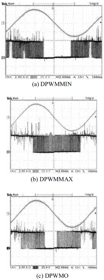
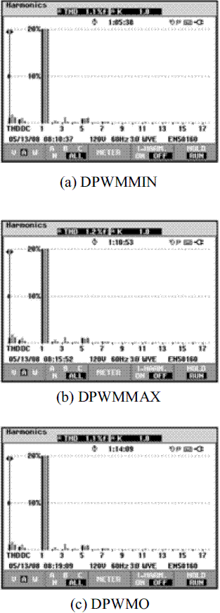
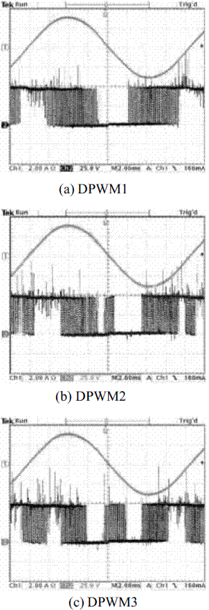
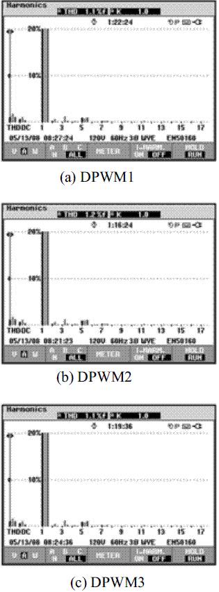
<body><![CDATA[<p><font face="Verdana" size="2">PWM master switch period selection: 800</font></p>      <p><font face="Verdana" size="2">With this set up the PWM circuitry is operating at 10 kHz switching frequency, and the registers for programming the PWM duty cycles use integers in the range [0 to 800] for duty cycles between 0&#37; and 100&#37;. <a href="#Figura9">Figures 9</a> to <a href="#Figura12">12</a> show the current, trigger signal and current harmonics content for phase <i>“a”</i> when the modulation methods DPWMMIN, DPWMMAX, DPWM0, DPWM1, DPWM2 and DPWM3 are applied to the power converter for a circular trajectory in the linear region with &#40;MI&#61;0.898&#41;. In general, as was to be expected, the current waveforms and harmonics content are almost the same in the six implemented modulation methods, but the trigger signals have different characteristics.</font></p>      <p><font face="Verdana" size="3"><b>Conclusions</b></font></p>     <p><font face="Verdana" size="2">Three basic methods, DPWMMIN, DPWMMAX and SVPWM using a parallelogram based mapping algorithm for producing per phase duty cycles, for references in &alpha;, &beta; coordinates have been proposed, and experimental results for DPWMMIN and DPWMMAX and other four combined methods, DPWM0, DPWM1, DPWM2 and DPWM3 have been presented in this work. The proposed modulation methods are especially suited for controllers requiring high dynamic response such as FOC, DTC, DPC, etc., and are easily adapted to be used in scalar controllers. An advantage of the proposed methods is that they employ the triangle intersection technique and the resulting duty cycles can be readily fed to standard carrierbased PWM modules.</font></p>     <p align="center"><font face="Verdana" size="2"><img src="/img/revistas/rfiua/n52/n52a14i36.gif" ><a name="Figura9"></a></font></p>       <p><font face="Verdana" size="2"><b>Figure 9</b> Experimental phase “a” current and power devices&rsquo; trigger signal for DPWMMIN, DPWMMAX and DPWM0 modulation methods implemented using the proposed algorithms</font></p>      <p align="center"><font face="Verdana" size="2"><img src="/img/revistas/rfiua/n52/n52a14i37.gif" ><a name="Figura10"></a></font></p>      <p><font face="Verdana" size="2"><b>Figure 10</b> Experimental phase “a” current harmonics content for DPWMMIN, DPWMMAX and DPWM0 modulation methods implemented using the proposed algorithms</font></p>     <p><font face="Verdana" size="2">The mathematical operations required by the algorithms are simple multiplications, additions, absolute values and comparisons, making them suitable to be implemented in low performance processors. The algorithms run in less than 2&mu;s, using less than 2&#37; of the control cycle defined in the test rig DSP controller [27]. This is a very important advantage when the proposed modulation strategies are used in modern applications where the overall control scheme represents a high computational</font></p>      <p align="center"><font face="Verdana" size="2"><img src="/img/revistas/rfiua/n52/n52a14i38.gif" ><a name="Figura11"></a></font></p>      ]]></body>
<body><![CDATA[<p><font face="Verdana" size="2"><b>Figure 11</b> Experimental phase “a” current and power devices&rsquo; trigger signal for DPWM1, DPWM2 and DPWM3 modulation methods implemented using the proposed algorithms</font></p>     <p><font face="Verdana" size="2">Load. Several modern modulation techniques can be obtained combining the use of DPWMMIN and DPWMMAX by properly selecting the areas for using each method. This approach also leads to a reduction in the computational burden of these modern modulation methods. The performance of the modulation methods has been verified with experimental tests, and the results are in good agreement with the theoretical analysis presented in this paper.</font></p>      <p align="center"><font face="Verdana" size="2"><img src="/img/revistas/rfiua/n52/n52a14i39.gif" ><a name="Figura12"></a></font></p>      <p><font face="Verdana" size="2"><b>Figure 12</b> Experimental phase “a” current harmonics content for DPWM1, DPWM2 and DPWM3 modulation methods implemented using the proposed algorithms</font></p>     <p><font face="Verdana" size="3"><b>References</b></font></p>     <!-- ref --><p><font face="Verdana" size="2">1. J. Zubek, A. Abbondanti, C. J. Norby. “Pulsewidth modulated inverter motor drives with improved modulation”. IEEE Trans. Ind. Applicat. Vol. 11. 1975. pp. 695&#45;703.</font>&nbsp;&nbsp;&nbsp;&nbsp;&nbsp;&nbsp;&nbsp;&nbsp;[&#160;<a href="javascript:void(0);" onclick="javascript: window.open('/scielo.php?script=sci_nlinks&ref=000108&pid=S0120-6230201000020001400001&lng=','','width=640,height=500,resizable=yes,scrollbars=1,menubar=yes,');">Links</a>&#160;]<!-- end-ref --><!-- ref --><p><font face="Verdana" size="2">2. G. B. Kliman, A. B. Plunkett. “Development of a modulation strategy for a PWM inverter drive”. IEEE Trans. Ind. Applicat. Vol. 15. 1979. pp. 72&#45;79.</font>&nbsp;&nbsp;&nbsp;&nbsp;&nbsp;&nbsp;&nbsp;&nbsp;[&#160;<a href="javascript:void(0);" onclick="javascript: window.open('/scielo.php?script=sci_nlinks&ref=000109&pid=S0120-6230201000020001400002&lng=','','width=640,height=500,resizable=yes,scrollbars=1,menubar=yes,');">Links</a>&#160;]<!-- end-ref --><!-- ref --><p><font face="Verdana" size="2">3. M. A. Boost, P. D. Ziogas. “State&#45;of&#45;the&#45;art carrier PWM techniques: A critical evaluation”. IEEE Trans. Ind. Applicat. Vol. 24. 1988. pp. 271&#45;280.</font>&nbsp;&nbsp;&nbsp;&nbsp;&nbsp;&nbsp;&nbsp;&nbsp;[&#160;<a href="javascript:void(0);" onclick="javascript: window.open('/scielo.php?script=sci_nlinks&ref=000110&pid=S0120-6230201000020001400003&lng=','','width=640,height=500,resizable=yes,scrollbars=1,menubar=yes,');">Links</a>&#160;]<!-- end-ref --><!-- ref --><p><font face="Verdana" size="2">4. J. Holtz. “Pulsewidth modulation&#45;a survey”. IEEE Trans. Ind. Electron. Vol. 39. 1992. pp. 410&#45;420.</font>&nbsp;&nbsp;&nbsp;&nbsp;&nbsp;&nbsp;&nbsp;&nbsp;[&#160;<a href="javascript:void(0);" onclick="javascript: window.open('/scielo.php?script=sci_nlinks&ref=000111&pid=S0120-6230201000020001400004&lng=','','width=640,height=500,resizable=yes,scrollbars=1,menubar=yes,');">Links</a>&#160;]<!-- end-ref --><!-- ref --><p><font face="Verdana" size="2">5. J. Holtz. “Pulsewidth modulation for electronic power conversion”. Proceedings of the IEEE. Vol. 82. 1994. pp. 1194&#45;1214.</font>&nbsp;&nbsp;&nbsp;&nbsp;&nbsp;&nbsp;&nbsp;&nbsp;[&#160;<a href="javascript:void(0);" onclick="javascript: window.open('/scielo.php?script=sci_nlinks&ref=000112&pid=S0120-6230201000020001400005&lng=','','width=640,height=500,resizable=yes,scrollbars=1,menubar=yes,');">Links</a>&#160;]<!-- end-ref --><!-- ref --><p><font face="Verdana" size="2">6. D. Chung, J. Kim, S. Sul. “Unified voltage modulation technique for real&#45;time three&#45;phase power conversion”. IEEE Trans. Ind. Applicat. Vol. 34. 1998. pp. 374&#45;380.</font>&nbsp;&nbsp;&nbsp;&nbsp;&nbsp;&nbsp;&nbsp;&nbsp;[&#160;<a href="javascript:void(0);" onclick="javascript: window.open('/scielo.php?script=sci_nlinks&ref=000113&pid=S0120-6230201000020001400006&lng=','','width=640,height=500,resizable=yes,scrollbars=1,menubar=yes,');">Links</a>&#160;]<!-- end-ref --><!-- ref --><p><font face="Verdana" size="2">7. D. Casadei, D. Dujic, E. Levi, G. Serra, A. Tani, L. Zarri. “General modulation strategy for seven&#45;phase inverters with independent control of multiple voltage space vectors”. IEEE Trans. Ind. Electron. Vol. 55. 2008. pp. 1921&#45;1932.</font>&nbsp;&nbsp;&nbsp;&nbsp;&nbsp;&nbsp;&nbsp;&nbsp;[&#160;<a href="javascript:void(0);" onclick="javascript: window.open('/scielo.php?script=sci_nlinks&ref=000114&pid=S0120-6230201000020001400007&lng=','','width=640,height=500,resizable=yes,scrollbars=1,menubar=yes,');">Links</a>&#160;]<!-- end-ref --><!-- ref --><p><font face="Verdana" size="2">8. H. V. der Broeck, H. Skudelny, G. Stanke. “Analysis and realization of a pulsewidth modulator based on voltage space vectors”. IEEE Trans. Ind. Applicat. Vol. 24. 1988. pp. 142&#45;150.</font>&nbsp;&nbsp;&nbsp;&nbsp;&nbsp;&nbsp;&nbsp;&nbsp;[&#160;<a href="javascript:void(0);" onclick="javascript: window.open('/scielo.php?script=sci_nlinks&ref=000115&pid=S0120-6230201000020001400008&lng=','','width=640,height=500,resizable=yes,scrollbars=1,menubar=yes,');">Links</a>&#160;]<!-- end-ref --><!-- ref --><p><font face="Verdana" size="2">9. A. M. Trzynadlowski, R. L. Kirlin, S. F. Legowski. “Space vector PWM technique with minimum switching losses and a variable pulse rate”. IEEE Trans. Ind. Electron.Vol. 44. 1997. pp. 173&#45;181.</font>&nbsp;&nbsp;&nbsp;&nbsp;&nbsp;&nbsp;&nbsp;&nbsp;[&#160;<a href="javascript:void(0);" onclick="javascript: window.open('/scielo.php?script=sci_nlinks&ref=000116&pid=S0120-6230201000020001400009&lng=','','width=640,height=500,resizable=yes,scrollbars=1,menubar=yes,');">Links</a>&#160;]<!-- end-ref --><!-- ref --><p><font face="Verdana" size="2">10. V. Blasko. “Analysis of a hybrid PWM based on modified space&#45;vector and triangle&#45;comparison methods”. IEEE Trans. Ind. Applicat. Vol. 33. 1997. pp. 756&#45;764.</font>&nbsp;&nbsp;&nbsp;&nbsp;&nbsp;&nbsp;&nbsp;&nbsp;[&#160;<a href="javascript:void(0);" onclick="javascript: window.open('/scielo.php?script=sci_nlinks&ref=000117&pid=S0120-6230201000020001400010&lng=','','width=640,height=500,resizable=yes,scrollbars=1,menubar=yes,');">Links</a>&#160;]<!-- end-ref --><!-- ref --><p><font face="Verdana" size="2">11. A. M. Hava, R. J. Kerkman, T. A. Lipo. “Carrierbased PWM&#45;VSI overmodulation strategies: Analysis, comparison, and design”. IEEE Trans. Power Electron. Vol. 13. 1998. pp. 674&#45;689. 1998.</font>&nbsp;&nbsp;&nbsp;&nbsp;&nbsp;&nbsp;&nbsp;&nbsp;[&#160;<a href="javascript:void(0);" onclick="javascript: window.open('/scielo.php?script=sci_nlinks&ref=000118&pid=S0120-6230201000020001400011&lng=','','width=640,height=500,resizable=yes,scrollbars=1,menubar=yes,');">Links</a>&#160;]<!-- end-ref --><!-- ref --><p><font face="Verdana" size="2">12. A. M. Hava, R. J. Kerkman, T. A. Lipo. “Simple analytical and graphical methods for carrier&#45;based PWM&#45;VSI drives”. IEEE Trans. Power Electron. 1999. Vol. 14. pp. 49&#45;61.</font>&nbsp;&nbsp;&nbsp;&nbsp;&nbsp;&nbsp;&nbsp;&nbsp;[&#160;<a href="javascript:void(0);" onclick="javascript: window.open('/scielo.php?script=sci_nlinks&ref=000119&pid=S0120-6230201000020001400012&lng=','','width=640,height=500,resizable=yes,scrollbars=1,menubar=yes,');">Links</a>&#160;]<!-- end-ref --><!-- ref --><p><font face="Verdana" size="2">13. J. Youm, B. Kwon. “An effective software implementation of the space&#45;vector modulation”. IEEE Trans. Ind. Electron. Vol. 46. 1999. pp. 866&#45;868. </font>&nbsp;&nbsp;&nbsp;&nbsp;&nbsp;&nbsp;&nbsp;&nbsp;[&#160;<a href="javascript:void(0);" onclick="javascript: window.open('/scielo.php?script=sci_nlinks&ref=000120&pid=S0120-6230201000020001400013&lng=','','width=640,height=500,resizable=yes,scrollbars=1,menubar=yes,');">Links</a>&#160;]<!-- end-ref --><!-- ref --><p><font face="Verdana" size="2">14. G. Narayanan, V. T. Ranganathan. “Extension of operation of space vector PWM strategies with low switching frequencies using different overmodulation algorithms”. IEEE Trans. Power Electron. Vol. 17. 2002. pp. 788&#45;798.</font>&nbsp;&nbsp;&nbsp;&nbsp;&nbsp;&nbsp;&nbsp;&nbsp;[&#160;<a href="javascript:void(0);" onclick="javascript: window.open('/scielo.php?script=sci_nlinks&ref=000121&pid=S0120-6230201000020001400014&lng=','','width=640,height=500,resizable=yes,scrollbars=1,menubar=yes,');">Links</a>&#160;]<!-- end-ref --><!-- ref --><p><font face="Verdana" size="2">15. L. Hao, X. Xiangning, X. Yonghai. “Study on the simplified algorithm of space vector PWM”. Proc. IEEE Fifth International Conference on Power Electronics and Drive Systems &#40;PEDS 2003&#41;. Singapore. 2003. pp. 877&#45;881.</font>&nbsp;&nbsp;&nbsp;&nbsp;&nbsp;&nbsp;&nbsp;&nbsp;[&#160;<a href="javascript:void(0);" onclick="javascript: window.open('/scielo.php?script=sci_nlinks&ref=000122&pid=S0120-6230201000020001400015&lng=','','width=640,height=500,resizable=yes,scrollbars=1,menubar=yes,');">Links</a>&#160;]<!-- end-ref --><!-- ref --><p><font face="Verdana" size="2">16. M. A. Jabbar, A. M. Khambadkone, Z. Yanfeng. “Space&#45;vector modulation in a two&#45;phase induction motor drive for constant&#45;power operation”. IEEE Trans. Ind. Electron. Vol. 51. 2004. pp. 1081&#45;1088.</font>&nbsp;&nbsp;&nbsp;&nbsp;&nbsp;&nbsp;&nbsp;&nbsp;[&#160;<a href="javascript:void(0);" onclick="javascript: window.open('/scielo.php?script=sci_nlinks&ref=000123&pid=S0120-6230201000020001400016&lng=','','width=640,height=500,resizable=yes,scrollbars=1,menubar=yes,');">Links</a>&#160;]<!-- end-ref --><!-- ref --><p><font face="Verdana" size="2">17. S. de Pablo, A. B. Rey, L. C. Herrero, J. M. Ruiz. “A simpler and faster method for SVM implementation”. Proceedings of the 2007 European Conference on Power Electronics and Applications. EPE 2007. pp. P1&#45;P9.</font>&nbsp;&nbsp;&nbsp;&nbsp;&nbsp;&nbsp;&nbsp;&nbsp;[&#160;<a href="javascript:void(0);" onclick="javascript: window.open('/scielo.php?script=sci_nlinks&ref=000124&pid=S0120-6230201000020001400017&lng=','','width=640,height=500,resizable=yes,scrollbars=1,menubar=yes,');">Links</a>&#160;]<!-- end-ref --><!-- ref --><p><font face="Verdana" size="2">18. G. Narayanan, D. Zhao, H. K. Krishnamurthy, R. Ayyanar, V. T. Ranganathan. “Space vector based hybrid PWM techniques for reduced current ripple”. IEEE Trans. Ind. Electron. Vol. 55. 2008. pp. 1614&#45; 1627.</font>&nbsp;&nbsp;&nbsp;&nbsp;&nbsp;&nbsp;&nbsp;&nbsp;[&#160;<a href="javascript:void(0);" onclick="javascript: window.open('/scielo.php?script=sci_nlinks&ref=000125&pid=S0120-6230201000020001400018&lng=','','width=640,height=500,resizable=yes,scrollbars=1,menubar=yes,');">Links</a>&#160;]<!-- end-ref --><!-- ref --><p><font face="Verdana" size="2">19. Z. Shu, J. Tang, Y. Guo, J. Lian. “An efficient SVPWM algorithm with low computational overhead for threephase inverters”. IEEE Trans. Power Electron. Vol. 22. 2007. pp. 1797&#45;1805.</font>&nbsp;&nbsp;&nbsp;&nbsp;&nbsp;&nbsp;&nbsp;&nbsp;[&#160;<a href="javascript:void(0);" onclick="javascript: window.open('/scielo.php?script=sci_nlinks&ref=000126&pid=S0120-6230201000020001400019&lng=','','width=640,height=500,resizable=yes,scrollbars=1,menubar=yes,');">Links</a>&#160;]<!-- end-ref --><!-- ref --><p><font face="Verdana" size="2">20. Z. Peroutka, T. Glasberger. “Comparison of methods for continuous transition of space vector PWM into six&#45;step mode”. Proceedings of the 12th international conference on power electronics and motion control EPE&#45;PEMC 2006. Portoroz. Slovenia. 2006. pp. 925&#45; 930.</font>&nbsp;&nbsp;&nbsp;&nbsp;&nbsp;&nbsp;&nbsp;&nbsp;[&#160;<a href="javascript:void(0);" onclick="javascript: window.open('/scielo.php?script=sci_nlinks&ref=000127&pid=S0120-6230201000020001400020&lng=','','width=640,height=500,resizable=yes,scrollbars=1,menubar=yes,');">Links</a>&#160;]<!-- end-ref --><!-- ref --><p><font face="Verdana" size="2">21. G. Narayanan, V. T. Ranganathan. “Trianglecomparison approach and space vector approach to pulsewidth modulation in inverter fed drives”. Journal of the Indian Institute of Science. Vol. 80. 2000. pp. 409&#45;427.</font>&nbsp;&nbsp;&nbsp;&nbsp;&nbsp;&nbsp;&nbsp;&nbsp;[&#160;<a href="javascript:void(0);" onclick="javascript: window.open('/scielo.php?script=sci_nlinks&ref=000128&pid=S0120-6230201000020001400021&lng=','','width=640,height=500,resizable=yes,scrollbars=1,menubar=yes,');">Links</a>&#160;]<!-- end-ref --><!-- ref --><p><font face="Verdana" size="2">22. D. Dujic, G. Grandi, M. Jones, E. Levi. “A space vector PWM scheme for multifrequency output voltage generation with multiphase voltage&#45;source inverters”. IEEE Trans. Ind. Electron. Vol. 55. 2008. pp. 1943&#45; 1955.</font>&nbsp;&nbsp;&nbsp;&nbsp;&nbsp;&nbsp;&nbsp;&nbsp;[&#160;<a href="javascript:void(0);" onclick="javascript: window.open('/scielo.php?script=sci_nlinks&ref=000129&pid=S0120-6230201000020001400022&lng=','','width=640,height=500,resizable=yes,scrollbars=1,menubar=yes,');">Links</a>&#160;]<!-- end-ref --><!-- ref --><p><font face="Verdana" size="2">23. A. M. Hava, S. Sul, R. J. Kerkman, T. A. Lipo. “Dynamic overmodulation characteristics of triangle intersection PWM methods”. IEEE Trans. Ind. Applicat. Vol. 35. 1999. pp. 896&#45;907.</font>&nbsp;&nbsp;&nbsp;&nbsp;&nbsp;&nbsp;&nbsp;&nbsp;[&#160;<a href="javascript:void(0);" onclick="javascript: window.open('/scielo.php?script=sci_nlinks&ref=000130&pid=S0120-6230201000020001400023&lng=','','width=640,height=500,resizable=yes,scrollbars=1,menubar=yes,');">Links</a>&#160;]<!-- end-ref --><!-- ref --><p><font face="Verdana" size="2">24. H. Lu, W. Qu, X. Cheng, Y. Fan, X. Zhang. “A novel PWM technique with two&#45;phase modulation”. IEEE Trans. Power Electron. Vol. 22. 2007. pp. 2403&#45;2409.</font>&nbsp;&nbsp;&nbsp;&nbsp;&nbsp;&nbsp;&nbsp;&nbsp;[&#160;<a href="javascript:void(0);" onclick="javascript: window.open('/scielo.php?script=sci_nlinks&ref=000131&pid=S0120-6230201000020001400024&lng=','','width=640,height=500,resizable=yes,scrollbars=1,menubar=yes,');">Links</a>&#160;]<!-- end-ref --><!-- ref --><p><font face="Verdana" size="2">25. K. Zhou, D. Wang. “Relationship between spacevector modulation and three&#45;phase carrier&#45;based PWM: A comprehensive analysis”. IEEE Trans. Ind. Electron. Vol. 49. 2002. pp. 186&#45;196.</font>&nbsp;&nbsp;&nbsp;&nbsp;&nbsp;&nbsp;&nbsp;&nbsp;[&#160;<a href="javascript:void(0);" onclick="javascript: window.open('/scielo.php?script=sci_nlinks&ref=000132&pid=S0120-6230201000020001400025&lng=','','width=640,height=500,resizable=yes,scrollbars=1,menubar=yes,');">Links</a>&#160;]<!-- end-ref --><!-- ref --><p><font face="Verdana" size="2">26. A. M. Hava, R. J. Kerkman, T. A. Lipo. “A highperformance generalized discontinuous pwm algorithm”. IEEE Trans. Ind. Applicat. Vol. 34. 1998. pp. 1059&#45;1071.</font>&nbsp;&nbsp;&nbsp;&nbsp;&nbsp;&nbsp;&nbsp;&nbsp;[&#160;<a href="javascript:void(0);" onclick="javascript: window.open('/scielo.php?script=sci_nlinks&ref=000133&pid=S0120-6230201000020001400026&lng=','','width=640,height=500,resizable=yes,scrollbars=1,menubar=yes,');">Links</a>&#160;]<!-- end-ref --><!-- ref --><p><font face="Verdana" size="2">27. J. Restrepo, M. I. Gim&eacute;nez, V. Guzm&aacute;n, J. M. Aller, A. Bueno, A. Mill&aacute;n. “PLATFORM III: A new version for the integrated test system for AC machine drives performance analysis”. Proceedings of the Fourth International Caracas Conference on Devices, Circuits and Systems. 2002. pp. 1036&#40;1&#41;&#45;1036&#40;6&#41;.</font>&nbsp;&nbsp;&nbsp;&nbsp;&nbsp;&nbsp;&nbsp;&nbsp;[&#160;<a href="javascript:void(0);" onclick="javascript: window.open('/scielo.php?script=sci_nlinks&ref=000134&pid=S0120-6230201000020001400027&lng=','','width=640,height=500,resizable=yes,scrollbars=1,menubar=yes,');">Links</a>&#160;]<!-- end-ref --><p><font face="Verdana" size="2">&#40;Recibido el 20 de febrero de 2009. Aceptado el 23 de septiembre de 2009&#41;</font></p>     <p><font face="Verdana" size="2"><sup>*</sup>Autor de correspondencia: tel&eacute;fono + 58 + 212 + 906 3637, fax: + 58 + 212 + 906 3631, correo electr&oacute;nico: <a href="mailto:restrepo@usb.ve">restrepo@usb.ve</a> &#40;J. Restrepo&#41;</font></p>      ]]></body><back>
<ref-list>
<ref id="B1">
<label>1</label><nlm-citation citation-type="journal">
<person-group person-group-type="author">
<name>
<surname><![CDATA[Zubek]]></surname>
<given-names><![CDATA[J]]></given-names>
</name>
<name>
<surname><![CDATA[Abbondanti]]></surname>
<given-names><![CDATA[A]]></given-names>
</name>
<name>
<surname><![CDATA[Norby]]></surname>
<given-names><![CDATA[C]]></given-names>
</name>
</person-group>
<article-title xml:lang="en"><![CDATA[Pulsewidth modulated inverter motor drives with improved modulation]]></article-title>
<source><![CDATA[IEEE Trans. Ind. Applicat]]></source>
<year>1975</year>
<volume>11</volume>
<page-range>695-703</page-range></nlm-citation>
</ref>
<ref id="B2">
<label>2</label><nlm-citation citation-type="journal">
<person-group person-group-type="author">
<name>
<surname><![CDATA[Kliman]]></surname>
<given-names><![CDATA[G. B]]></given-names>
</name>
<name>
<surname><![CDATA[Plunkett]]></surname>
<given-names><![CDATA[A. B]]></given-names>
</name>
</person-group>
<article-title xml:lang="en"><![CDATA[Development of a modulation strategy for a PWM inverter drive]]></article-title>
<source><![CDATA[IEEE Trans. Ind. Applicat]]></source>
<year>1979</year>
<volume>15</volume>
<page-range>72-79</page-range></nlm-citation>
</ref>
<ref id="B3">
<label>3</label><nlm-citation citation-type="journal">
<person-group person-group-type="author">
<name>
<surname><![CDATA[Boost]]></surname>
<given-names><![CDATA[M. A]]></given-names>
</name>
<name>
<surname><![CDATA[Ziogas]]></surname>
<given-names><![CDATA[P. D]]></given-names>
</name>
</person-group>
<article-title xml:lang="en"><![CDATA[State-of-the-art carrier PWM techniques: A critical evaluation]]></article-title>
<source><![CDATA[IEEE Trans. Ind. Applicat]]></source>
<year>1988</year>
<volume>24</volume>
<page-range>271-280</page-range></nlm-citation>
</ref>
<ref id="B4">
<label>4</label><nlm-citation citation-type="journal">
<person-group person-group-type="author">
<name>
<surname><![CDATA[Holtz]]></surname>
<given-names><![CDATA[J]]></given-names>
</name>
</person-group>
<article-title xml:lang="en"><![CDATA[Pulsewidth modulation-a survey]]></article-title>
<source><![CDATA[IEEE Trans. Ind. Electron]]></source>
<year>1992</year>
<volume>39</volume>
<page-range>410-420</page-range></nlm-citation>
</ref>
<ref id="B5">
<label>5</label><nlm-citation citation-type="journal">
<person-group person-group-type="author">
<name>
<surname><![CDATA[Holtz]]></surname>
<given-names><![CDATA[J]]></given-names>
</name>
</person-group>
<article-title xml:lang="en"><![CDATA[Pulsewidth modulation for electronic power conversion]]></article-title>
<source><![CDATA[Proceedings of the IEEE]]></source>
<year>1994</year>
<volume>82</volume>
<page-range>1194-1214</page-range></nlm-citation>
</ref>
<ref id="B6">
<label>6</label><nlm-citation citation-type="journal">
<person-group person-group-type="author">
<name>
<surname><![CDATA[Chung]]></surname>
<given-names><![CDATA[D]]></given-names>
</name>
<name>
<surname><![CDATA[Kim]]></surname>
<given-names><![CDATA[J]]></given-names>
</name>
<name>
<surname><![CDATA[Sul]]></surname>
<given-names><![CDATA[S]]></given-names>
</name>
</person-group>
<article-title xml:lang="en"><![CDATA[Unified voltage modulation technique for real-time three-phase power conversion]]></article-title>
<source><![CDATA[IEEE Trans. Ind. Applicat]]></source>
<year>1998</year>
<volume>34</volume>
<page-range>374-380</page-range></nlm-citation>
</ref>
<ref id="B7">
<label>7</label><nlm-citation citation-type="journal">
<person-group person-group-type="author">
<name>
<surname><![CDATA[Casadei]]></surname>
<given-names><![CDATA[D]]></given-names>
</name>
<name>
<surname><![CDATA[Dujic]]></surname>
<given-names><![CDATA[D]]></given-names>
</name>
<name>
<surname><![CDATA[Levi]]></surname>
<given-names><![CDATA[E]]></given-names>
</name>
<name>
<surname><![CDATA[Serra]]></surname>
<given-names><![CDATA[G]]></given-names>
</name>
<name>
<surname><![CDATA[Tani]]></surname>
<given-names><![CDATA[A]]></given-names>
</name>
<name>
<surname><![CDATA[Zarri]]></surname>
<given-names><![CDATA[L]]></given-names>
</name>
</person-group>
<article-title xml:lang="en"><![CDATA[General modulation strategy for seven-phase inverters with independent control of multiple voltage space vectors]]></article-title>
<source><![CDATA[IEEE Trans. Ind. Electron]]></source>
<year>2008</year>
<volume>55</volume>
<page-range>1921-1932</page-range></nlm-citation>
</ref>
<ref id="B8">
<label>8</label><nlm-citation citation-type="journal">
<person-group person-group-type="author">
<name>
<surname><![CDATA[der Broeck]]></surname>
<given-names><![CDATA[H. V]]></given-names>
</name>
<name>
<surname><![CDATA[Skudelny]]></surname>
<given-names><![CDATA[H]]></given-names>
</name>
<name>
<surname><![CDATA[Stanke]]></surname>
<given-names><![CDATA[G]]></given-names>
</name>
</person-group>
<article-title xml:lang="en"><![CDATA[Analysis and realization of a pulsewidth modulator based on voltage space vectors]]></article-title>
<source><![CDATA[IEEE Trans. Ind. Applicat]]></source>
<year>1988</year>
<volume>24</volume>
<page-range>142-150</page-range></nlm-citation>
</ref>
<ref id="B9">
<label>9</label><nlm-citation citation-type="journal">
<person-group person-group-type="author">
<name>
<surname><![CDATA[Trzynadlowski]]></surname>
<given-names><![CDATA[A. M]]></given-names>
</name>
<name>
<surname><![CDATA[Kirlin]]></surname>
<given-names><![CDATA[R. L]]></given-names>
</name>
<name>
<surname><![CDATA[Legowski]]></surname>
<given-names><![CDATA[S. F]]></given-names>
</name>
</person-group>
<article-title xml:lang="en"><![CDATA[Space vector PWM technique with minimum switching losses and a variable pulse rate]]></article-title>
<source><![CDATA[IEEE Trans. Ind. Electron]]></source>
<year>1997</year>
<volume>44</volume>
<page-range>173-181</page-range></nlm-citation>
</ref>
<ref id="B10">
<label>10</label><nlm-citation citation-type="journal">
<person-group person-group-type="author">
<name>
<surname><![CDATA[Blasko]]></surname>
<given-names><![CDATA[V]]></given-names>
</name>
</person-group>
<article-title xml:lang="en"><![CDATA[Analysis of a hybrid PWM based on modified space-vector and triangle-comparison methods]]></article-title>
<source><![CDATA[IEEE Trans. Ind. Applicat]]></source>
<year>1997</year>
<volume>33</volume>
<page-range>756-764</page-range></nlm-citation>
</ref>
<ref id="B11">
<label>11</label><nlm-citation citation-type="journal">
<person-group person-group-type="author">
<name>
<surname><![CDATA[Hava]]></surname>
<given-names><![CDATA[A. M]]></given-names>
</name>
<name>
<surname><![CDATA[Kerkman]]></surname>
<given-names><![CDATA[R. J]]></given-names>
</name>
<name>
<surname><![CDATA[Lipo]]></surname>
<given-names><![CDATA[T]]></given-names>
</name>
</person-group>
<article-title xml:lang="en"><![CDATA[Carrierbased PWM-VSI overmodulation strategies: Analysis, comparison, and design]]></article-title>
<source><![CDATA[IEEE Trans. Power Electron]]></source>
<year>1998</year>
<volume>13</volume>
<page-range>674-689</page-range></nlm-citation>
</ref>
<ref id="B12">
<label>12</label><nlm-citation citation-type="journal">
<person-group person-group-type="author">
<name>
<surname><![CDATA[Hava]]></surname>
<given-names><![CDATA[A. M]]></given-names>
</name>
<name>
<surname><![CDATA[Kerkman]]></surname>
<given-names><![CDATA[R. J]]></given-names>
</name>
<name>
<surname><![CDATA[Lipo]]></surname>
<given-names><![CDATA[T. A]]></given-names>
</name>
</person-group>
<article-title xml:lang="en"><![CDATA[Simple analytical and graphical methods for carrier-based PWM-VSI drives]]></article-title>
<source><![CDATA[IEEE Trans. Power Electron]]></source>
<year>1999</year>
<volume>14</volume>
<page-range>49-61</page-range></nlm-citation>
</ref>
<ref id="B13">
<label>13</label><nlm-citation citation-type="journal">
<person-group person-group-type="author">
<name>
<surname><![CDATA[Youm]]></surname>
<given-names><![CDATA[J]]></given-names>
</name>
<name>
<surname><![CDATA[Kwon]]></surname>
<given-names><![CDATA[B]]></given-names>
</name>
</person-group>
<article-title xml:lang="en"><![CDATA[An effective software implementation of the space-vector modulation]]></article-title>
<source><![CDATA[IEEE Trans. Ind. Electron]]></source>
<year>1999</year>
<volume>46</volume>
<page-range>866-868</page-range></nlm-citation>
</ref>
<ref id="B14">
<label>14</label><nlm-citation citation-type="journal">
<person-group person-group-type="author">
<name>
<surname><![CDATA[Narayanan]]></surname>
<given-names><![CDATA[G]]></given-names>
</name>
<name>
<surname><![CDATA[Ranganathan]]></surname>
<given-names><![CDATA[V. T]]></given-names>
</name>
</person-group>
<article-title xml:lang="en"><![CDATA[Extension of operation of space vector PWM strategies with low switching frequencies using different overmodulation algorithms]]></article-title>
<source><![CDATA[IEEE Trans. Power Electron]]></source>
<year>2002</year>
<volume>17</volume>
<page-range>788-798</page-range></nlm-citation>
</ref>
<ref id="B15">
<label>15</label><nlm-citation citation-type="confpro">
<person-group person-group-type="author">
<name>
<surname><![CDATA[Hao]]></surname>
<given-names><![CDATA[L]]></given-names>
</name>
<name>
<surname><![CDATA[Xiangning]]></surname>
<given-names><![CDATA[X]]></given-names>
</name>
<name>
<surname><![CDATA[Yonghai]]></surname>
<given-names><![CDATA[X]]></given-names>
</name>
</person-group>
<source><![CDATA[Study on the simplified algorithm of space vector PWM]]></source>
<year></year>
<conf-name><![CDATA[Fifth International Conference on Power Electronics and Drive Systems (PEDS 2003)]]></conf-name>
<conf-date>2003</conf-date>
<conf-loc>Singapore </conf-loc>
<page-range>877-881</page-range></nlm-citation>
</ref>
<ref id="B16">
<label>16</label><nlm-citation citation-type="journal">
<person-group person-group-type="author">
<name>
<surname><![CDATA[Jabbar]]></surname>
<given-names><![CDATA[M. A]]></given-names>
</name>
<name>
<surname><![CDATA[Khambadkone]]></surname>
<given-names><![CDATA[A. M]]></given-names>
</name>
<name>
<surname><![CDATA[Yanfeng]]></surname>
<given-names><![CDATA[Z]]></given-names>
</name>
</person-group>
<article-title xml:lang="en"><![CDATA[Space-vector modulation in a two-phase induction motor drive for constant-power operation]]></article-title>
<source><![CDATA[IEEE Trans. Ind. Electron]]></source>
<year>2004</year>
<volume>51</volume>
<page-range>1081-1088</page-range></nlm-citation>
</ref>
<ref id="B17">
<label>17</label><nlm-citation citation-type="confpro">
<person-group person-group-type="author">
<name>
<surname><![CDATA[de Pablo]]></surname>
<given-names><![CDATA[S]]></given-names>
</name>
<name>
<surname><![CDATA[Rey]]></surname>
<given-names><![CDATA[A. B]]></given-names>
</name>
<name>
<surname><![CDATA[Herrero]]></surname>
<given-names><![CDATA[L. C]]></given-names>
</name>
<name>
<surname><![CDATA[Ruiz]]></surname>
<given-names><![CDATA[J. M]]></given-names>
</name>
</person-group>
<source><![CDATA[A simpler and faster method for SVM implementation]]></source>
<year></year>
<conf-name><![CDATA[ 2007 European Conference on Power Electronics and Applications]]></conf-name>
<conf-date>2007</conf-date>
<conf-loc> </conf-loc>
<page-range>P1-P9</page-range></nlm-citation>
</ref>
<ref id="B18">
<label>18</label><nlm-citation citation-type="journal">
<person-group person-group-type="author">
<name>
<surname><![CDATA[Narayanan]]></surname>
<given-names><![CDATA[G]]></given-names>
</name>
<name>
<surname><![CDATA[Zhao]]></surname>
<given-names><![CDATA[D]]></given-names>
</name>
<name>
<surname><![CDATA[Krishnamurthy]]></surname>
<given-names><![CDATA[H. K]]></given-names>
</name>
<name>
<surname><![CDATA[Ayyanar]]></surname>
<given-names><![CDATA[R]]></given-names>
</name>
<name>
<surname><![CDATA[Ranganathan]]></surname>
<given-names><![CDATA[V. T]]></given-names>
</name>
</person-group>
<article-title xml:lang="en"><![CDATA[Space vector based hybrid PWM techniques for reduced current ripple]]></article-title>
<source><![CDATA[IEEE Trans. Ind. Electron]]></source>
<year>2008</year>
<volume>55</volume>
<page-range>1614- 1627</page-range></nlm-citation>
</ref>
<ref id="B19">
<label>19</label><nlm-citation citation-type="journal">
<person-group person-group-type="author">
<name>
<surname><![CDATA[Shu]]></surname>
<given-names><![CDATA[Z]]></given-names>
</name>
<name>
<surname><![CDATA[Tang]]></surname>
<given-names><![CDATA[J]]></given-names>
</name>
<name>
<surname><![CDATA[Guo]]></surname>
<given-names><![CDATA[Y]]></given-names>
</name>
<name>
<surname><![CDATA[Lian]]></surname>
<given-names><![CDATA[J]]></given-names>
</name>
</person-group>
<article-title xml:lang="en"><![CDATA[An efficient SVPWM algorithm with low computational overhead for threephase inverters]]></article-title>
<source><![CDATA[IEEE Trans. Power Electron]]></source>
<year>2007</year>
<volume>22</volume>
<page-range>1797-1805</page-range></nlm-citation>
</ref>
<ref id="B20">
<label>20</label><nlm-citation citation-type="confpro">
<person-group person-group-type="author">
<name>
<surname><![CDATA[Peroutka]]></surname>
<given-names><![CDATA[Z]]></given-names>
</name>
<name>
<surname><![CDATA[Glasberger]]></surname>
<given-names><![CDATA[T]]></given-names>
</name>
</person-group>
<source><![CDATA[Comparison of methods for continuous transition of space vector PWM into six-step mode]]></source>
<year></year>
<conf-name><![CDATA[12 international conference on power electronics and motion control]]></conf-name>
<conf-date>2006</conf-date>
<conf-loc> </conf-loc>
<page-range>925- 930</page-range></nlm-citation>
</ref>
<ref id="B21">
<label>21</label><nlm-citation citation-type="journal">
<person-group person-group-type="author">
<name>
<surname><![CDATA[Narayanan]]></surname>
<given-names><![CDATA[G]]></given-names>
</name>
<name>
<surname><![CDATA[Ranganathan]]></surname>
<given-names><![CDATA[V. T]]></given-names>
</name>
</person-group>
<article-title xml:lang="en"><![CDATA[Trianglecomparison approach and space vector approach to pulsewidth modulation in inverter fed drives]]></article-title>
<source><![CDATA[Journal of the Indian Institute of Science]]></source>
<year>2000</year>
<volume>80</volume>
<page-range>409-427</page-range></nlm-citation>
</ref>
<ref id="B22">
<label>22</label><nlm-citation citation-type="journal">
<person-group person-group-type="author">
<name>
<surname><![CDATA[Dujic]]></surname>
<given-names><![CDATA[D]]></given-names>
</name>
<name>
<surname><![CDATA[Grandi]]></surname>
<given-names><![CDATA[G]]></given-names>
</name>
<name>
<surname><![CDATA[Jones]]></surname>
<given-names><![CDATA[M]]></given-names>
</name>
<name>
<surname><![CDATA[Levi]]></surname>
<given-names><![CDATA[E]]></given-names>
</name>
</person-group>
<article-title xml:lang="en"><![CDATA[A space vector PWM scheme for multifrequency output voltage generation with multiphase voltage-source inverters]]></article-title>
<source><![CDATA[IEEE Trans. Ind. Electron]]></source>
<year>2008</year>
<volume>55</volume>
<page-range>1943- 1955</page-range></nlm-citation>
</ref>
<ref id="B23">
<label>23</label><nlm-citation citation-type="journal">
<person-group person-group-type="author">
<name>
<surname><![CDATA[Hava]]></surname>
<given-names><![CDATA[A. M]]></given-names>
</name>
<name>
<surname><![CDATA[Sul]]></surname>
<given-names><![CDATA[S]]></given-names>
</name>
<name>
<surname><![CDATA[Kerkman]]></surname>
<given-names><![CDATA[R. J]]></given-names>
</name>
<name>
<surname><![CDATA[Lipo]]></surname>
<given-names><![CDATA[T. A]]></given-names>
</name>
</person-group>
<article-title xml:lang="en"><![CDATA[Dynamic overmodulation characteristics of triangle intersection PWM methods]]></article-title>
<source><![CDATA[IEEE Trans. Ind. Applicat]]></source>
<year>1999</year>
<volume>35</volume>
<page-range>896-907</page-range></nlm-citation>
</ref>
<ref id="B24">
<label>24</label><nlm-citation citation-type="journal">
<person-group person-group-type="author">
<name>
<surname><![CDATA[Lu]]></surname>
<given-names><![CDATA[H]]></given-names>
</name>
<name>
<surname><![CDATA[Qu]]></surname>
<given-names><![CDATA[W]]></given-names>
</name>
<name>
<surname><![CDATA[Cheng]]></surname>
<given-names><![CDATA[X]]></given-names>
</name>
<name>
<surname><![CDATA[Fan]]></surname>
<given-names><![CDATA[Y]]></given-names>
</name>
<name>
<surname><![CDATA[Zhang]]></surname>
<given-names><![CDATA[X]]></given-names>
</name>
</person-group>
<article-title xml:lang="en"><![CDATA[A novel PWM technique with two-phase modulation]]></article-title>
<source><![CDATA[IEEE Trans. Power Electron]]></source>
<year>2007</year>
<volume>22</volume>
<page-range>2403-2409</page-range></nlm-citation>
</ref>
<ref id="B25">
<label>25</label><nlm-citation citation-type="journal">
<person-group person-group-type="author">
<name>
<surname><![CDATA[Zhou]]></surname>
<given-names><![CDATA[K]]></given-names>
</name>
<name>
<surname><![CDATA[Wang]]></surname>
<given-names><![CDATA[D]]></given-names>
</name>
</person-group>
<article-title xml:lang="en"><![CDATA[Relationship between spacevector modulation and three-phase carrier-based PWM: A comprehensive analysis]]></article-title>
<source><![CDATA[IEEE Trans. Ind. Electron]]></source>
<year>2002</year>
<volume>49</volume>
<page-range>186-196</page-range></nlm-citation>
</ref>
<ref id="B26">
<label>26</label><nlm-citation citation-type="journal">
<person-group person-group-type="author">
<name>
<surname><![CDATA[Hava]]></surname>
<given-names><![CDATA[A. M]]></given-names>
</name>
<name>
<surname><![CDATA[Kerkman]]></surname>
<given-names><![CDATA[R. J]]></given-names>
</name>
<name>
<surname><![CDATA[Lipo]]></surname>
<given-names><![CDATA[T. A]]></given-names>
</name>
</person-group>
<article-title xml:lang="en"><![CDATA[A highperformance generalized discontinuous pwm algorithm]]></article-title>
<source><![CDATA[IEEE Trans. Ind. Applicat]]></source>
<year>1998</year>
<volume>34</volume>
<page-range>1059-1071</page-range></nlm-citation>
</ref>
<ref id="B27">
<label>27</label><nlm-citation citation-type="confpro">
<person-group person-group-type="author">
<name>
<surname><![CDATA[Restrepo]]></surname>
<given-names><![CDATA[J]]></given-names>
</name>
<name>
<surname><![CDATA[Giménez]]></surname>
<given-names><![CDATA[M]]></given-names>
</name>
<name>
<surname><![CDATA[Guzmán]]></surname>
<given-names><![CDATA[V]]></given-names>
</name>
<name>
<surname><![CDATA[Aller]]></surname>
<given-names><![CDATA[J. M]]></given-names>
</name>
<name>
<surname><![CDATA[Bueno]]></surname>
<given-names><![CDATA[A]]></given-names>
</name>
<name>
<surname><![CDATA[Millán]]></surname>
<given-names><![CDATA[A]]></given-names>
</name>
</person-group>
<source><![CDATA[PLATFORM III: A new version for the integrated test system for AC machine drives performance analysis]]></source>
<year></year>
<conf-name><![CDATA[Fourth International Caracas Conference on Devices, Circuits and Systems]]></conf-name>
<conf-date>2002</conf-date>
<conf-loc> </conf-loc>
<page-range>1036(1)-1036(6)</page-range></nlm-citation>
</ref>
</ref-list>
</back>
</article>