PROPIEDADES ELÉCTRICAS DE NANO-MULTICAPAS DE Cr/CrN PRODUCIDAS POR LA TÉCNICA DE SPUTTERING CON MAGNÉTRÓN DESBALANCEADO
DIANA MARITZA MARULANDA CARDONA
Departamento de Ingeniería Mecánica y Mecatrónica, Universidad Nacional de Colombia. dmaritzamc@gmail.com
JHON JAIRO OLAYA FLOREZ
Departamento de Ingeniería Mecánica y Mecatrónica, Universidad Nacional de Colombia. jjolaya@unal.edu.co
Received for review November 24th, 2009; accepted December 2nd, 2010; final version December 23rd, 2010
]]>ABSTRACT: Chromium nitride (CrN) films have been applied to several steels as protective coatings against wear and corrosion due to their excellent mechanical properties and corrosion resistance, and in the electronic field these films are commonly used due to their low electrical resistivity. However, it has been found that multilayers combining metal/ceramic films could enhance mechanical and electrical properties compared with their monolayer counterparts, due to the higher amount and interaction between interfaces. In this work, Cr/CrN nano-multilayers have been produced through the unbalanced magnetron sputtering technique with three different degrees of unbalance, in order to study the influence of this parameter on electrical properties. Cr/CrN multilayers with approximately 1 mm of total thickness and a bilayer period (L) of 200 nm, 100 nm, and 20 nm were produced at room temperature on H13 steel and silicon (100); and their microstructure and electrical properties as a function of the magnetic field were evaluated. The phase formation was characterized through x-ray diffraction, and results presented (111) and (200) preferred orientations for all the multilayers. Cross section images were obtained through scanning electron microscopy and a multilayer structure can be clearly seen.
KEY WORDS: Multilayers, unbalanced magnetron sputtering, UBM, Cr/CrN, resistivity
RESUMEN: Películas de nitruro de cromo (CrN) se han aplicado como recubrimientos protectores contra el desgaste y la corrosión debido a sus excelentes propiedades mecánicas y alta resistencia a la corrosión, y en el campo electrónico debido a su baja resistividad. Sin embargo, se ha encontrado que las multicapas que combinan películas metal/cerámico podrían mejorar las propiedades en comparación a sus contrapartes en monocapa debido al aumento e interacción entre interfaces. En este trabajo se produjeron nano-multicapas de Cr/CrN a través de la técnica de sputtering con magnetrón desbalanceado con tres grados de desbalanceo diferentes para estudiar la influencia de este parámetro en las propiedades eléctricas. Se crecieron multicapas con un espesor total de aproximadamente 1 mm y un período de bicapa (L) de 200 nm, 100 nm y 20 nm. Las multicapas se produjeron a temperatura ambiente sobre acero H13 y silicio (100) y se estudió su microestructura y las propiedades eléctricas en función del campo magnético. La formación de fases se caracterizó a través de Difracción de Rayos X y los resultados muestran las orientaciones (111) y (200) para todas las multicapas. Se obtuvieron imágenes de la sección transversal a través de Microscopía Electrónica de Barrido y los resultados muestran la formación de una estructura en multicapas.
PALABRAS CLAVE:Multicapas, sputtering con magnetrón desbalanceado, UBM, Cr/CrN, resistividad.
1. INTRODUCTION
Chromium/chromium nitride multilayer coatings have received attention in recent years due to their high level of hardness and corrosion resistance [1-5] which are higher than those of their monolayer counterparts, especially because the interfaces present in multilayers act as barriers to crack propagation and dislocation movement, and the re-nucleation presented in these structures reduces pores resulting in better corrosion resistance [6-8]. Cr and CrN multilayer coatings could also find an application as materials for low-resistivity diffusion barriers because the presence of interfaces would block diffusion through grain boundaries [7] and the grain size reduction which is common for this kind of structures [9,10] would form long diffusion paths through grain boundaries.
Physical vapor deposition (PVD) techniques are commonly used to produce high quality coatings at the nanometer scale [11-14], especially the techniques based on sputter deposition. The unbalanced magnetron (UBM) sputtering technique has gained attention due to its superior performance compared to conventional balanced magnetron [15]. With UBM, the level of unbalance of the magnetron varies the magnetic field in such way that the field lines are not confined to the target region but are also directed towards the substrate resulting in a high ionic current on the substrate and a high flux of coating atoms [16]. The ionic bombarding produced on the substrate modifies adatoms mobility [17] during film growth and hence the film properties are also modified [18].
The level of unbalance of a magnetron can be estimated using a coefficient of geometrical unbalance KG, according to [19]:
]]> (1)
(1) Where R is the average radius of the erosion zone and Z (Bz=0) is the distance from the target surface to the point on the axis of the magnetron where the magnetic field changes its direction [19], that is, where Bz component takes a value of zero.
In this study, Cr/CrN nano-multilayers were produced using the UBM technique by varying the level of unbalance of the magnetron, and its influence on the in-plane resistivity was studied in order to evaluate this kind of structure for low-resistivity barrier diffusion applications.
2. EXPERIMENTAL SETUP
2.1. Multilayer deposition
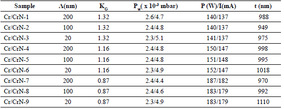
The nano-multilayers of Cr/CrN were deposited by means of the UBM technique in a vacuum chamber that has an unbalanced magnetron GENCOA sputter VT 100 which allows for one to vary the magnetic field through the variation in the number of turns (NV) of a millimeter screw which changes the distance between the magnets assembly and the target. An increment in NV corresponds to enlarging the distance between the central magnet and the target and, consequently, modifying the magnetic field configuration. The average radius of the erosion zone (R) and Z(Bz=0) shown in equation (1) were measured by using a portable teslameter Phywe with a Hall effect probe, and KG was calculated according to these data as a function of Nv. The coefficient of geometrical unbalance varied inversely with the level of unbalance of the magnetron: a high KG value implied a low level of unbalance of the magnetron and vice versa. The multilayers were produced with three different KG values (KG = 1.32, 1.16, and 0.87) as shown in Table 1.
Table 1. Deposition conditions: period (L), unbalance coefficient (KG), working pressure (Pw), discharge power (P), discharge current (I), thickness (t)
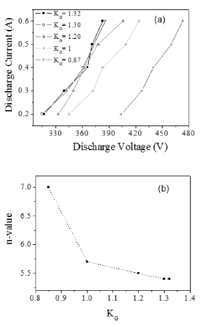
The magnetron current-voltage characteristic was estimated to determine variations in efficiency with the unbalance coefficient. A sputtering system has a current-voltage (I-V) characteristic that behaves as (at constant pressure) [20]. Exponent n reflects how well the electrons are confined by the magnetic trap in the race track. An optimum magnetron should give an nvalue which is typically around 5-9 [20]. Figure 1(a) shows the current-voltage characteristic for argon-nitrogen discharge using a Cr target and the n-values (Fig. 1[b]) as a function of KG were determined according to the current-voltage values. Figure 1(b) illustrates that the efficiency of the magnetron increases for low KG values, this means, a higher electron density is reached for KG = 0.87 (and therefore a higher level of unbalance of the magnetron), while lower electron density is obtained for KG = 1.32.
]]>
Commercial AISI H13 tool steel of 0.32-0.45 C, 0.8-1.20 Si, 0.20-0.50 Mn, 4.75-5.5 Cr, 0.8-1.20 V, 1.10-1.75 Mo, Fe balance (wt%) composition, and silicon (100) were used as substrates. Steel samples were polished using sandpaper from 100 to 1200, pretreated by quenching (1000-1025 °C) and tempering (175-315 °C) and finally, they were mirror polished. Before introducing the substrates in the deposition chamber, they were ultrasonically cleaned in acetone and alcohol in sequence and dried in flowing compressed air.
Multilayers were produced with a bilayer period of 200 nm, 100 nm, and 20 nm, and approximately 1 mm of total thickness. The base pressure was less than 9x10⁻⁴ Pa. All the multilayers were grown at room temperature and the sample target distance was set to 5 cm while Ar and N2 flow rates were set to 9 standard cubic centimeters per minute (sccm) and 3 sccm, respectively. The substrate was floating without any external bias. Deposition conditions are summarized in Table 1.
2.2. Multilayers Characterization
Identification of crystallographic phases and preferential orientations of the multilayers was done by x-ray diffraction (XRD) using an XPertPro Panalytical system under conditions of 6° grazing incident, 90°/s spinning velocity and monochromatized CuKa radiation. The cross-sectional morphology of the multilayers grown on Si (100) was studied using a FEIKUANTA 200 scanning electron microscope (SEM).
The four point probe (FPP) method was used to obtain in-plane resistivity of the multilayers. Sheet resistance values were taken and resistivity was calculated according to the expression [21,22]:
 (2)
(2)
Where r is the resistivity (mW-cm), Rs is the sheet resistance (ohms per square), and t is the multilayer thickness. The FPP was placed in contact with the film surface and the current was applied across the outer two probes while voltage drop was measured across the two inner probes. Four assumptions that are important for consistent good measurements were taken into account [23]: 1) the spacing between probe tips was the same between each probe tip, 2) the contact pressure on all four probe tips was uniform, 3) the edge of the sample was at least 10 times the spacing from the nearest probe tip, and 4) the thickness of the sample was less than 4 times the spacing between probe tips.
A Lucas Signatone four-point probe head with tungsten carbide tips and 0.0012 inch tip radius was used. Spacing between tips was 0.040 inches and the pressure applied was 45 grams.
]]> Six sets of measurements were made for each multilayer applying a current of 1, 2, 4, 6, 8, and 10 mA, and the average for sheet resistance was calculated. Cr/CrN multilayers total thickness (t) was measured with a Veeco Dektak 150 profilometer, and the results are summarized in Table 1.
3. RESULTS AND DISCUSSION
Structural characterization
Results for high angle XRD are shown in Fig. 2 for multilayers grown with L = 200 nm. The SEM results show a clearly defined layered structure for multilayers with L = 200 nm (Fig. 3[a]) and L = 100 nm (Fig. 3[b]). For multilayers with L = 20 nm (not shown), it was not possible to obtain a clear image due to the resolution of the microscope used. The in-plane resistivity results are shown in Fig. 4. As can be seen, lower resistivity values were found for multilayers grown with KG = 0.87. This could be due to the higher plasma efficiency reached in this configuration, where electrons are confined to the target region and they are lost in fewer amounts to the chamber walls producing dense plasma on the substrate region.
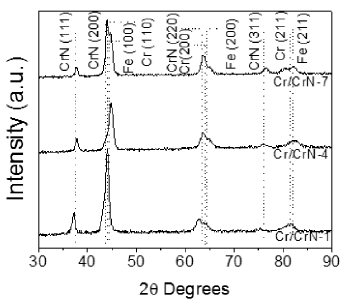
Figure 2. XRD pattern for multilayers grown with L = 200 nm
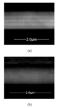
Figure 3. Cross section SEM micrographs of the multilayers grown with (a) L = 200 nm, (b) L = 100 nm and KG = 1.32
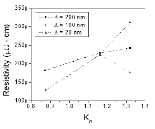 ]]>
Figure 4. In- plane resistivity as a function of KG. The dotted lines serve as a guide to the eye.
]]>
Figure 4. In- plane resistivity as a function of KG. The dotted lines serve as a guide to the eye.
In turn, the ionization efficiency in plasma results in considerably higher ion currents at the substrate, and therefore, the ion flux increases as the degree of unbalance increases [24]. The ion bombardment induces adatom mobility producing microstructural changes and therefore denser coatings with fewer defects. These microstructural changes have been studied for different coatings such as Al, Zr, W [25], and TiN [26], among others.
Resistivity in a thin film arises due to electron scattering by phonons, point defects, impurities, grain boundaries, and film surfaces and interfaces [27]. As denser films (fewer defects inside grains) are produced for KG = 0.87, lower resistivity values are obtained. As in the in-plane measurement the applied current passes through the lower resistivity layers (i.e. Cr layers), there is no noteworthy influence of the interfaces on the resistivity (Cr has a bulk resistivity of 13 mWcm while CrN has a bulk resistivity of 640 mW-cm [28]).
The resistivity reached a value of approximately 225 mW-cm for all the multilayers grown with KG = 1.16, and higher resistivity values were found for the multilayer grown with KG = 1.32 and L = 20 nm, where lower plasma efficiency is presented.
4. CONCLUSIONS
In this work, Cr/CrN nano-multilayers were produced through the unbalanced magnetron sputtering technique with three different levels of unbalance, and the influence of this parameter on electrical properties was evaluated. Results show that a higher degree of unbalance of the magnetron produces lower resistivity for all the multilayer periods, which could indicate that denser films are produced due to the increase in mobility as a result of the higher plasma efficiency reached in this configuration.
ACKNOWLEDGMENTS
This research has been financially supported by the Instituto Colombiano para el desarrollo de la Ciencia y la Tecnología Francisco José de Caldas-COLCIENCIAS, through project 1101-479-22003 CT 531-2008, the Fundación Para la Promoción de la Ciencia y la Tecnología, through a project under contract 200814 and the Dirección de Investigación de la Universidad Nacional de Colombia sede Bogotá, through project 11109.
]]>REFERENCES
[1] R. Bayón, A. Igartua, X.Fernández, R. Martínez, R.J. Rodríguez, J.A. García, A. de Frutos, M.A. Arenas, J.de Damborenea, Tribology International, 42 (2009) 591-599. [ Links ]
[2] J. Stockemer a, R. Winand, P. Vanden Brande, Surf. Coat. Technol., 115 (1999) 230-233. [ Links ]
[3] E. Martínez, J. Romero, A. Lousa and J. Esteve, J. Phys. D: Appl. Phys, 35 (2002) 1880-1883. [ Links ]
[4] S. Kaciulis, A. Mezzi, G. Montesperelli, F. Lamastra, M. Rapone, F. Casadei, T. Valente, G. Gusmano, Surf. Coat. Technol., 201 (2006) 313-319. [ Links ]
[5] M. Kot, W.A. Rakowski, L. Major, R. Major, J. Morgiel, Surf. Coat. Technol., 202 (2008) 3501-3506. [ Links ]
[6] J.J. Olaya, Recubrimientos de nitruros metálicos depositados con la técnica de espurreo asistido con campos magnéticos variables, PhD. Thesis, Instituto de Investigaciones en Materiales, UNAM, México, 2005. [ Links ]
[7] R. Hubler, Surf. Coat. Technol., 116-119, pp. 1116-1122, (1999). [ Links ]
[8] A. Leyland, A. Mathews, Surf. Coat. Technol. 70, pp.19-25, (1994). [ Links ]
[9] E. Zart, Acta Mater. 46, 5611 (1998). [ Links ]
[10] M. Flores, S. Muhl, L. Huerta, E. Andrade, Surf. Coat. Technol, 200, 1315 (2005). [ Links ]
[11] A. Conde, C. Navas, A.B. Cristóbal, J. Housden, J. de Damborenea, Surf. Coat. Technol., 201 (2006) 2690-2695. [ Links ]
[12] A. Barata, L. Cunha, C. Moura, Thin Solid Films 398 -399 (2001) 501-506. [ Links ]
[13] C. Gautier, H. Moussaoui, F. Elstner, J. Machet, Surf. and Coat. Technol., 86-87 (1996) 254-262. [ Links ]
[14] Wei-Yu Ho, Cheng-Hsun Hsu, Dung-Hau Huang, Yen-Chun Lin, Chi-Lung Chang, Da-Yung Wang, Surf. & Coat. Technol. 200 (2005) 1303 - 1309. [ Links ]
[15] J.J. Olaya, S.E. Rodil, S. Muhl, E. Sánchez, Thin Solid Films 474 (2005) 119- 126. [ Links ]
[16] P.J. Kelly, R.D. Arnell, Vacuum, 56 (2000) 159-172. [ Links ]
[17] J.J. Olaya, S.E. Rodil, S. Muhl, L. Huerta, Surf. Coat. Technol., 200 (2006) 5743-5750. [ Links ]
[18] P.J. Kelly, R.D. Arnell, Surf. Coat. Technol., 108-109 (1998) 317-322. [ Links ]
[19] I.V. Svadkovski, D.A. Golosov, S.M. Zavatskiy, Vacuum 68 (2003) 283-290. [ Links ]
[20] Rossnagel S M and Kaufman H R, J. Vac. Sci. Technol. A 6 (1988) 223 [ Links ]
[21] Dieter, K. Schroder, Semiconductor Material and Device Characterization, John Wiley and Sons, Inc, New York, 1998. [ Links ]
[22] H. J. Wondergem, A. Heger, J. J. van Den Broek, Thin Solid Films 249, 6 (1994). [ Links ]
[23] L. B. Valdes in Proceedings of the IRE 42 (1954) 420. [ Links ]
[24] Jun Zhou, Zhe Wu, and Zhanhe Liu, Journal of University of Science and Technology Beijing Volume 15, Number 6, December 2008, Page 775. [ Links ]
[25] P.J. Kelly, R.D. Arnell, Surf. Coat. Technol., 97 (1997) 595-602. [ Links ]
[26] M. Zlatanovic, R. Belosevac, N. Popovic, A. Kunosic, Surf. Coat. Technol., 106 (1998) 150-155. [ Links ]
[27] D. Schumacher, Surface Scattering Experiments with Conduction Electrons, Springer-Verlag, Berlin, 1993. [ Links ]
[28] Bhushan B, Gupta BK, in Handbook of tribology, McGraw-Hill, New York (1991) p. 4.54. [ Links ] ]]>