


 English (pdf)
 Article in xml format
 Article references
 Send this article by e-mail
 Cited by SciELO
  Cited by Google
  Similars in
SciELO
Similars in
SciELO  Similars in Google
 Permalink
1. Introduction
Colombia currently has best energy infrastructure and is third with the highest quality of energy supply at the generation, transmission, distribution, and commercialization level for countries in the Central and South American region [1]. Energy is primarily generated with hydroelectric resources (responsible for 69% of the country's energy production) with a potential of 90,000 MW, gas production (responsible for 24.8% of the country's energy production) which contributes 967 million cubic meters a day, and oil reserves with a production of 647,000 barrels of crude oil per day [2]. Even so, in the case of the hydroelectric sector, there are environmental impacts such as loss of flora and fauna, alteration of the environment, deterioration of water quality, modification of habitat and aquatic biodiversity, erosion, sedimentation, and greenhouse gas effects [3].
As a solution to the problem, non-habitual renewable energies have taken an important role in generating large-scale electricity production. Solar energy utilizes solar radiation applied to a photovoltaic module made up of cells capable of transforming incident light energy into DC electrical energy. Since the conventional electrical network is based on AC voltage, a conversion from direct current to alternating current is required to take advantage of photovoltaic solar systems [4].
For this reason, it is necessary to implement high performance DC/AC inverters with high functionality indices that correspond to the demands required by society regarding this type of technology. The area of power electronics has the capacity to design, develop, and implement devices that provide maximum efficiency in energy conversion, avoid significant losses, and give rise to systems with high performance, capacity, and quality.
This document presents a detailed implementation of a high efficiency (91.5%) Current Source Inverter (CSI) using Silicon Carbide SiC semiconductor technology and Unipolar Sinusoidal Pulse Width Modulation (SPWM). This technology provides easy implementation and great results in the performance of the inverter. It is worth mentioning that this type of modulation is not widely developed for this type of CSIs.
1.1. Current source inverter
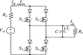
The monophasic inverter CSI in a bridge type configuration is composed of four switching devices and the inductance in series with the input source and a capacitor at the bridge output. The input inductance acts as a constant current source that is subsequently modulated to obtain the sinusoidal signal at the output [5,6]. The switching devices are composed by three quadrant semiconductors. These include a MOSFET and a diode which is ideal for the application since the inverter must withstand bidirectional currents and positive unidirectional voltages [7]. The topology of the CSI inverter is shown in Fig. 1. and includes the switching devices S1, S2, S3, and S4.
1.2. Inverter design
1.2.1. Sizing of passive components
The modulation used for the operation of the inverter is called unipolar sinusoidal pulse width modulation (SPWM). It has a triangular carrier signal and two reference sinusoidal signals out, phased 180° between them [8,9]. These signals will be determined by the duty cycle that each delivery D, 1-D, D1, and 1-D1 sends to the switching devices S1, S2, S3, and S4, respectively.
Considering the small and large signal analysis to identify the inductor and capacitor values for the CSI inverter by the unipolar SPWM modulation [10], eq. (1)-(2) represented the inductor and capacitor values respectively, taking into consideration the stablished parameters in Table 1, for an input and output power of 200 W.
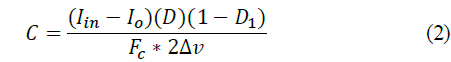
Replacing, the values in the table for those in the equation, an inductor and a capacitor value of L ≈ 0.2 H y C ≈ 20 μF was obtained.
1.2.2. Proportional resonant controller design
A proportional resonant PR controller was chosen since it offers advantages such as ease of implementation and low harmonic content against perturbances in the load [11,12]. Table 2 shows the parameters of the design of the controller considering its transfer function presented in eq. (3).
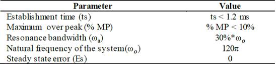
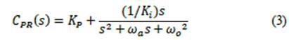
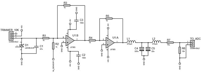
Through different mathematical calculations, the damping factor and the natural frequency of the second order system is equalized with both the desired characteristic polynomial and the characteristic closed-loop polynomial, resulting in the controller constants Kp = 0.04183 and Ki =252.29. Since the controller must be discretized to be implemented in a microcontroller, the bilinear transformation or Tustin method [13] was used to calculate the values. Eq. (3) and eq. (4) were used, where T is the sample time of the controller, U[n] is the actual control signal in discrete time, and E(n) is the actual error as a result of the subtraction between the reference signal and the sensed voltage signal at the output.
2. Implementation
2.1.1. Passive inverter bridge components
A metallized polypropylene capacitor was selected as the voltage storage element. It is characterized by operating with a high frequency of currents in addition to having a low parasitic impedance [14,15]. This capacitor supports a maximum voltage of 470 V and in practice, two 10 μF capacitors connected in parallel were used.
A specifically designed inductor using an E-type ferrite laminated core, AWG 13 copper wiring, a maximum current of 8 A, an effective area equivalent to 3.42 mm2, 598 windings, and a GAP length equal to 5.13 mm.
2.2. Semiconductor devices
2.2.1. Selection of switching devices
The switching devices used were MOSFETs and diodes which must quickly respond to the control signals due the frequency of the modulation while also able to withstand a minimum voltage of 170 Vp and a current of 2.35 A. The CREE™ MOSFET C3M0065090D, is manufactured of silicon carbide SiC that allows on and off times close to 11 and 9 ns respectively while having a maximum switching frequency of 90.9 MHz, the ability to withstand a maximum voltage of 900 V between the drain and source, a voltage of 19 V to -8 V between the gate and source, a drain current of 36 A, and a small resistance value of Rdson of 65 Ω [16].
The CREE™ diode C3D16060D also uses silicon carbide SiC and has a recovery time of zero, a forward voltage Vd of 1.5 V, a maximum reverse voltage of 600 V, maximum current of 22 A, and resistance of 18 Ω [17].
2.2.2. Isolation and driver circuit
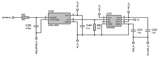
The circuits using MOSFETs controlled by microcontrollers must have an isolation stage between the devices that drive AC signals and the digital circuit that sends the signals for the on/off of the switching devices. An ACPL-4800 optocoupler was used which is comprised of Gallium Arsenide Phosphide GaAsP along with a Schmitt trigger gate that allows for fast switching in state transitions. It has a power range of 4.5 V to 20 V, a maximum pulse width distortion equal to 250 ns, a maximum current at a 25 mA output, and a maximum propagation delay of 150 ns [18]. In practical terms, in the input of the optocoupler will enter a 3.3 V signal generated by the microcontroller. Eq. (5) shows the calculation of the resistor connected between the internal diode of the optocoupler and the generated signal by the microcontroller taking into consideration that the optocoupler supports a maximum current of 8 mA which is less than what is specified in the datasheet.

A IXD-609-PI driver was selected for the MOSFETs on/off signals. This driver delivers a maximum current of 9 A at the output, has maximum propagation delay of 35 ns, and can deliver and receive a trigger signal between -5 V and the positive voltage with which the device is powered [19]. The driver was powered using between 15 V and -5 V; however, in eq. (6) the resistance value between the controller output and the MOSFET gate is shown assuming a current of 1 A at the output of the driver and an effective voltage of a square signal from 15 V to -5 V. The resistor is included to reduce parasitic oscillation by the gate capacitance [20,21].

LM7805, LM7905, and isolated sources of 15 V and -15 V were used to supply the isolation and driver circuits to maintain balance and symmetry in the energization for each trigger stage of the four MOSFETs. Fig. 2 shows the isolated stage and control stage for the switching of each MOSFET taking into consideration the optocoupler and driver mentioned with the calculated resistors. Additionally, different capacitors recommended by the manufacturer were included to eliminate noise. The label “EPWM1A” is the control signal sent by the microcontroller and the label “S1” is the trigger signal sent to the MOSFET’s gate. This circuit was replicated three more times in the design of the PCB.
2.2.3. Voltage sensing
To sense the voltage signal at the inverter output considering its sinusoidal shape, the differential voltage probes P5200A Series of the brand Tektronix® were used. These probes work at a maximum bandwidth of 50 MHz, can sense a maximum voltage of 1300 V and have a configurable attenuation of x50 V or x500 V [22]. For the connection of the probes to the circuit a BNC connector with an impedance of 50 Ω connector was used, this connector sends +-10 mV/V at the output.
Because the ADC input of the microcontroller should handle voltages referenced to ground and only detect positives voltage values, an offset with an accurate voltage source is necessary in the measure delivered by the differential probes. The LM336 is IC that is characterized by has a low consumption current of 400 uA to 10 mA and provide a fixed voltage supply of 2.5 V through a zener diode; this device has a dynamic impedance of 0.2 Ω and should be supply with 5 V [23].
To carry out the conditioning of the signal sensed by the differential probe, LF353 operational amplifiers in inverter adder mode were used to obtain the signal in phase with the real signal measured. Due to the high commutations generated in the reading of the output signal seen experimentally, the design of a LCL filter was necessary, this type of filter presents attenuation of 60 dB/decade from the resonance frequency and that with the aid of the capacitor the switching harmonics from the current deposited in the load are absorbed [24]. The resonance frequency of the LCL filter ωres is represented by eq. (7), where ωres should be place between 10 times the fundamental frequency of the signal to filter ω1 and half of the switching frequency ωs, to avoid problems of resonance in the fundamental frequency of the signal to measure [24].

Having as fundamental frequency 60 Hz and switching frequency 18 kHz, a resonant frequency was selected for the filter equal to 4 kHz. Eq. (8) shows the value of capacitor considering the resonance frequency ωres, the input inductance L and the output inductance Ls [24], assuming values of 470 μH and 570 μH respectively.
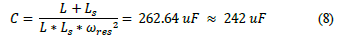
Finally, a 12 kΩ resistor was added in the output of the LCL filter, to decrease the current coming from the sensing stage. Fig. 3. shows the complete circuit used for the measure of the voltage at the output of the inverter, considering the conditioning and filtering stage designed, where the label “04_SENSOR” is the output of the BNC connector of the differential probes.
2.3. Generation of control signals and measurement acquisition
Due the accuracy that should be handled in the generation of the SPWM control signals, a Texas Instruments TMS320F28379D microcontroller was selected as the control device. This device has dual cores, an operation frequency of 200 MHz, 1024 kB of memory flash, 64 I/O pins, a 16-bit and 12-bit ADC converter, and specified peripherals for the generation of high resolution PWM signals [25]. The peripheral accessory, Enhanced Pulse Width Modulation EPWM, enabled the generation of the unipolar SPWM modulation for the trigger signals of the MOSFETs, the Analog Digital Converter ADC, and reading the voltage measurement. This type of microcontroller, in addition to having a high frequency of operation in the processing of information, is widely used in applications related to electronic power systems that require the precise switching of controlled devices [26].
3. Inverter printed circuit
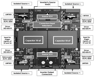
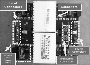
The development of the printed circuit took into account: the design of short and thick paths to reduce the losses generated by the commutation, placing capacitors as close as possible to power devices to reduce losses, ground insulation through perforations on the plate between the ends of the different integrated circuits in order to avoid external noise in radio frequency, the use of shielded wires to avoid false commutations that may affect the state transitions in the switches, and the generation of ground planes in order to eliminate parasitic impedance effects between the digital and power stage [27]. Fig 4 shows the 3D model of the top layer of the printed circuit of the inverter, where the supply devices, optocouplers, trigger drivers, inductance connectors, and capacitors were placed.
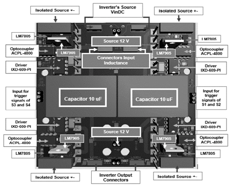
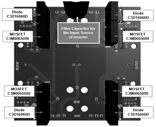
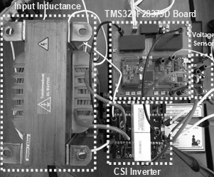
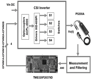
Fig. 5 shows the bottom layer of the printed circuit, where the MOSFETs, diodes of the inverter bridge, and an additional electrolytic capacitor to filter the supply of the inverter bridge in the power stage were placed. Fig. 6-7 shows the top layer and bottom layer of the real printed circuit, respectively. Fig. 8 shows the general diagram of the inverter implementation identifying the control signals generated by the microcontroller identified as: EPWM1A, EPWM1B, EPWM2A, and EPWM2B and the peripherals that control the switches S1, S2, S3, and S4 respectively. The general connection of the optocouplers, control drivers, and the signal sensed by the differential probes in the port A0 of the microcontroller are shown as well. Fig. 9 shows the general system developed for the CSI inverter.
The configuration of the output ports for the open loop programming of the SPWM signals was performed using the peripherals EPWM1A, EPWM1B, EPWM2A, and EPWM2B in mode Up-Down. This allowed the generation of internal triangular signals from the intern counters of the processor. Delays and overlaps were also configured to prevent false commutations on the switches and the activation of the complement signals D and D1. A CPU timer interrupt was configurated every 4 μs to always compare the sinusoidal signal and the triangular signal with a high quality of processing and avoid delays in the principal algorithm. After the configuration was done, the principal algorithm consisted of performing an overlap of 33 μs in the generated signals and configuring the frequency of 14 kHz to the carrier signal. In the CPU timer interrupt, the positive and negative sinusoidal reference signals are generated taking into consideration their modulation index Ma. These signals have a frequency of 60 Hz that depends on a variable t which will gradually increase its value to obtain a better shape and resolution in the generation of the sinusoidal signal at the output of the inverter.
For the programming in a closed loop, the 12-bit ADC configuration by the input AN0 was added. This calculated the actual value of the error and later the subtraction between the reference signa which was internally programmed into the microcontroller by a sine function with an amplitude of 170 Vp and the measured voltage signal. Afterwards, the comparison between the characteristic equation of the controller shows in eq. (4) was programmed and later the control signal from the previous step was added. Finally, the control signal was compared with the carrier signal to generate de SPWM modulation with feedback control.
4. Experimental results
4.1. Open loop testing
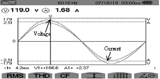
The behavior of the inverter was evaluated at a power of 200 W at the output. Fig. 10 shows the voltage and current waveforms at the output of the inverter given by the Power Quality Analyzer PowerPad III for a lineal load of 72 Ω. The switching frequency used was 9 kHz and the modulation index was 0.74. A value of 119 Vrms and 1.68 Arms was obtained with a frequency of 60.10 Hz in the output of the inverter.
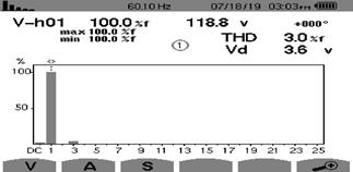
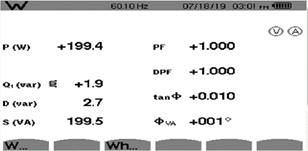
Figs. 11-12 shows the voltage harmonic content at the output of the inverter and the delivered power to the load, respectively. There was a harmonic distortion factor of 3%, an average value practically equal to zero and an excellent sine waveform by the circuit to deliver the power provided in the design.
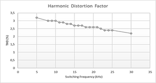
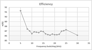
Tests were performed having a fixed modulation index of 0.74 and varying the switching frequency on the switches. This allowed the behavior of the circuit regarding the harmonic distortion factor of the voltage at the output and its efficiency to be observed. Figs. 13-14 show the behavior curves against frequency variations in the switches. By decreasing the harmonic distortion factor when the switching frequency increases resulted in a change of less than 2.5%. The efficiency decreases when the switching frequency increases due the switches having a greater transition between the on/off state and generating an increase in the temperature of the MOSFETs and diodes and consequently, more losses.
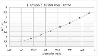
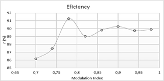
Figs. 15-16 shows the behavior curves against the modulation index versus the harmonic distortion factor and efficiency respectively. An increase in the harmonic distortion factor at the output and an improvement in the efficiency of the circuit close to 90% when the modulation index is increased can be observed. Therefore, the overall result is that the efficiency of the circuit and the harmonic distortion factor at the output increases.
4.2. Close loop testing
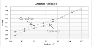
A voltage sweep was performed varying the load from 72 Ω to 100 Ω, with 4 Ω intervals using both open-loop and closed-loop systems with the PR controller proposed in eq. (3). Fig. 17 shows the behavior curve of the controlled circuit attenuated in terms of load variation versus output voltage Vorms.
Source: The Authors.
Figure. 17 Load variation versus output voltage Vorms in a closed loop and considering the load variations.
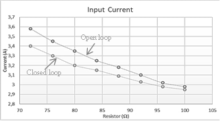
Fig. 18 shows that the circuit with a control presents a smaller decrease in slope compared to the uncontrolled input current. There is a better response with the controller regarding the manipulation of the input current since the modulation index is directly related to both the input current and the output current of the circuit.
Source: The Authors.
Figure. 18 Load variation versus input current Iinrms in a closed loop and considering the load variations.
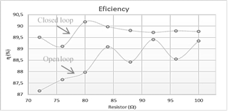
Finally, Fig. 19 shows a greater linearity of efficiency in the circuit implemented with a control with variations between 89.1% to 90.5% throughout the variation of the load. This differs to the open loop circuit which has its maximum peak efficiency of 89.4%
5. Conclusion
According to tests carried out using frequency sweeps and an open-loop modulation index; CSI inverters were found to have a decrease in efficiency as a result of an increase in switching frequency. As the efficiency decreases the harmonic distortion factor decreases since there is a proportional relationship between the efficiency compensation, harmonic distortion factor, and switching frequency for this inverter. The CSI inverter is a switched system; therefore, it has a non-linear behavior that is reflected in the high demand that the controller must have. However, the controller responded correctly to the values close to the operating point, i.e., loads very close to 72 Ω. If there are greater loads, the implementation of a more robust controller may be necessary. The CSI inverter met the agreed specifications regarding amplitude values and capacity delivered to different types of loads. Similarly, the harmonic distortion factor reached the recommended standard IEEE Std 519 ™-2014 for allowable harmonic content in the operation of systems that handle AC voltage, being less than 8% for systems that handle voltages below 1 kV peak. The unipolar SPWM modulation in this type of inverter allowed us to verify the feasibility of its implementation in such a way that future research may result in better performance due to the different energy conversion processes according to the converter topology that was implemented. Finally, its reliability is guaranteed for a subsequent connection to the network.

