


Services on Demand
Journal
Article
 English (pdf)
 Article in xml format
 Article references
 Send this article by e-mail
Indicators
-
 Cited by SciELO
 -
 Access statistics
Related links
-
 Cited by Google
 -
 Similars in
SciELO
Similars in
SciELO -
 Similars in Google
Share

 Permalink
TecnoLógicas
Print version ISSN 0123-7799On-line version ISSN 2256-5337
TecnoL. vol.20 no.39 Medellín May/Aug. 2017
Artículo de investigación/Research article
Fabrication of mems devices – a scanning micro mirror case study
Fabricación de sistemas MEMS – un caso de estudio en la fabricación de un micro-espejo
Artur Zarzycki1, Wiktor L. Gambin2, Sylwester Bargiel3, and Christophe Goreck4
1 PhD en Ingeniería Mecánica, Ingeniería Electromecánica, Grupo de Investigación en Automática, Electrónica y Ciencias Computacionales, Línea Sistemas de Control y Robótica, Facultad de Ingenierías, Instituto Tecnológico Metropolitano, Medellín-Colombia, arturzarzycki@itm.edu.co
2 PhD en Mecánica Aplicada, Instytut Mikromechaniki i Fotoniki, Zaklad Mechaniki Stosowanej, Politechnika Warszawska, Warsaw – Poland, wgambin@mchtr.pw.edu.pl
3 PhD en Ingeniería Electrónica, Département Micro Nano Sciences & Systèmes, MOEMS, Institut FEMTO-ST, University Bourgogne Franche-Comté, Besançon – France, sylwester.bargiel@femto-st.fr
4 PhD en Ingeniería de Microsistemas, Département Micro Nano Sciences &Systèmes, MOEMSInstitut FEMTO-ST, University Bourgogne Franche-Comté, Besançon – France christophe.gorecki@femto-st.fr
Fecha de recepción: 31 de marzo de 2017/ Fecha de aceptación: 15 de mayo de 2017
Como citar / How to cite
A. Zarzycki, W. L. Gambin, S. Bargiel and C. Gorecki, “Fabrication of MEMS devices – a scanning micro mirror case study”, TecnoLógicas, vol. 20, no. 39, 2017.
Abstract
This paper presents the working principle, design, and fabrication of a silicon-based scanning micromirror with a new type of action mechanism as an example of MEMS (Micro-Electro-Mechanical Systems). Micromirrors can be found in barcode readers as well as micro-projectors, optical coherence tomography, or spectrometers adjustable filters. The fabrication process of the device prompted us to describe and discuss the problems related to the manufacture of MEMS. The article starts with some terminology and a brief introduction to the field of microsystems. Afterwards, the concept of a new scanning micromirror is explained. The device is operated by two pairs of thermal bimorphs. A special design enables to maintain a constant distance from the center of the mirror to the light source during the scanning process. The device was implemented in a one degree-of-freedom micromirror and a two degree-of-freedom micromirror. The fabrication process of both types is described. For each case, a different type of substrate was used. The first type of substrate was a standard silicon wafer; the second one, SOI (Silicon-On-Insulator). The process with the first one was complicated and caused many problems. Replacing this substrate with SOI solved some of the issues, but did not prevent new ones from arising. Nevertheless, the SOI substrate produces much better results and it is preferable to manufacture this type of MEMS devices.
Keywords: MEMS, microsystems, microfabrication, microtechnology, microscanner, scanning micromirror.
Resumen
Este trabajo muestra un mecanismo de acción, un diseño y una fabricación de un nuevo dispositivo de escaneo - un micro-espejo. Los micro-espejos se pueden encontrar en los lectores de códigos de barras, así como en los micro proyectores, en sistemas de tomografía óptica coherente, o en los filtros ajustables de espectrómetros. El proceso de formación del nuevo dispositivo nos llevó a describir y discutir los problemas relacionados con la fabricación de MEMS (sistemas microelectrónicos). En primer lugar, se da una terminología y una breve introducción al campo de los microsistemas. A continuación, se explica un concepto del nuevo micro-espejo de escanéo. El dispositivo es accionado por dos pares de actuadores termo-bimorfos. Un diseño especial permite mantener la distancia constante desde el centro del espejo a la fuente de luz durante el proceso de escaneo. El dispositivo se implementó en dos versiones: un micro-espejo con un grado de libertad y un micro-espejo con dos grados de libertad. Se describe un proceso de fabricación para los dos tipos del dispositivo que utiliza dos tipos diferentes de sustrato. El primer tipo de sustrato corresponde a una oblea de silicio estándar, el segundo substrato corresponde a un SOI (Silicon-On-Insulator). El proceso con la oblea de silicio estándar fue complicado y causó muchos problemas. Cambiar el sustrato a SOI ayudó a resolver algunos de ellos, pero no permitió evitar algunos nuevos. Sin embargo, el sustrato SOI da mejores resultados y se encuentra que es preferible fabricar dispositivos MEMS de este tipo.
Palabras clave: MEMS, microsistemas, micro fabricación, micro tecnología, micro-escáner, micro espejo de escaneo.
1. Introduction
MEMS is an acronym which stands for Micro-Electro-Mechanical Systems and refers to miniature devices in which at least one of the characteristic dimensions is in the range of micrometers. The MEMS devices are compromise between different domains, however, mostly they merge mechanical and electrical systems. Intensive development of microsystem technology has caused that MEMS devices are present almost everywhere around us. Smartphones equipped with microgyroscope, cars where microaccelerometers are used for airbag activation, or personal gas sensors are just few examples of MEMS applications.
A particular group of MEMS is MOEMS (Micro-Opto-Electro-Mechanical Systems). MOEMS in fact is MEMS combined with micro-optics which involves sensing or manipulating optical signals on a very small size scale, using integrated mechanical, optical and electrical systems. The good example of MOEMS application is a matrix of thousands of microscopic, movable mirrors. For instance, such matrix is a hearth of an image projector where is responsible for image creation.
A key type of MEMS are microactuators, which are generally responsible for moving or controlling a mechanism or other system. They are often defined as microtransducers since actuators convert one form of energy into mechanical one. The most common actuators convert electrical energy into mechanical one by engaging a variety of physical phenomena. Hence, there are actuators such as: electrostatic, piezoelectric, electromagnetic, thermome-chanical, etc.
Detailed analysis of actuator types and micromirrors based on them one can find in [1]-[2]. Microscanners based on electrostatic actuation make the most extensive group of micros-canners, since electrostatic actuation is the simplest one. Essentially it based on attraction of two electrodes with contrary polarity. Such actuators are characterized by very high work frequency – grate advantageous for scanning micromirrors. Unfortunately, the deflection angle of the mirror is usually very limited. In addition, electrostatic actuation needs quite large voltage and is affected by pull-in effect.
Microscanners with piezoelectric actuation are characterized by fast response, low power consumption and can achieve large deflection angle of the. As negative aspects of piezoelectric actuators one must mention complicated fabrication process and hysteresis effect of material.
Micromirrors moved by electromagnetic actuators can realize large scan angle. Movement of the mirror is due to large attraction and repulsion forces generated by the actuator. However, electromagnetic scanners are large because magnetic actuation requires large electromagnets. The large size of the devices leads to great weight of movable parts and, in result, to small operating frequency.
Thermomechanical actuators stand out among the other for their large travel range and high force per unit volume ratio. They are easy to fabricate and integrate. That is why this type of actuation method has been chosen to the design presented in the paper. Unfortunately, electrothermal actuators have issue of high power consumption and slow response. Nevertheless, the second issue can be mitigated by proper construction of the whole device.
A thermobimorph actuator is an example of one of them. It has usually a form of cantilever composed of two layers which differ in coefficient of thermal expansion (CTE). The bottom layer (the passive one) has a lower CTE, whereas the top layer (the active one) has a higher CTE. Due to mismatch between the CTEs of the materials, the bimorphs after their fabrica-tion, curl out-of-plane and take a form of an arc of a circle. Thermobimorphs subjected to high temperature became strait, whereas when the high temperature is removed, they bent backwards and take again a form of an arc of a circle. They can achieve a large displacement with medium power consumption and their fabrication process is relatively simple.
It is very important to notice that MEMS is not just about the miniaturization of mechanical components or making things out of silicon. MEMS refers also to a manufacturing technology. It is a paradigm for designing and creating complex mechanical devices and systems as well as their integrated electronics using batch fabrication techniques.
The process of MEMS fabrication, called simply microfabrications, is derived from IC manufacturing technology and is supplemented by its own processes.
Microfabrication involves two basic methods: bulk micromaching and surface micromachining. In the bulk micromachining, the substrate is selectively removed (etched) to create three dimensional microstructures. Wet etching is a predominant technique here. However, sometimes it is necessary to etch throughout the substrate and in such case dry etching is preferred. In turn, surface micromachining is a process which is based on depositing layers on the substrate and then modifying them, e.g. by etching. The procedure of depositing and etching can be repeated several times. The extra layers might be, for instance, insulators, semiconductors, metals, polymers. Very often, to obtain desired structure or device, both bulk and surface micromachining technique are used alternately.
In microfabrication process, independently on the fabrication method, a substrate, a photomask or a set of photomasks and photolithography process play key rules. As a substrate a single-crystal silicon wafer is mostly preferred. It is dictated not only by its well-established electronic properties but also, or even rather, by its excellent mechanical properties. A pho-tomask is a transparent fused silica plate covered with a patterned UV-light absorbing thin layer, usually it is a chrome film. The pattern is transferred onto the substrate in photolithography process. The process is slightly similar to traditional photographic processing: first, the substrate is covered by UV-sensitive resist (so-called photoresist), next, the photoresist layer is covered by a photomask and exposed to UV-light. After exposure the photoresist is developed. Depending on the type of photoresist either the exposed areas are removed – this is in case of positive photoresist, or not-exposed ones - this is in case of negative photoresist.
It should be emphasized that the above mentioned techniques are just rough overview of the microfabrication process. Each project requires individual approach in which many aspects must be taken into account. Working on a new MEMS device it is necessary to work simultaneously on two: its design analysis and its manufacture, since both issues are very strongly coupled to each other. For instance, when analyzing particular materials for a device one must keep in mind if there is technological compatibility between them, i.e. if processing one material does not affect the previous or next one. On the other hand, different techniques of microfabrication give different material properties (such as mechanical, electrical, optical), which in return must be taken into account during design analysis.
Following parts of the article describe issues related to design, technology and fabrication of a new scanning micromirror, driven by thermobimorph actuators. The device is named shortly microscanner.
2. Materials and methods
2.1 Microscanner concept
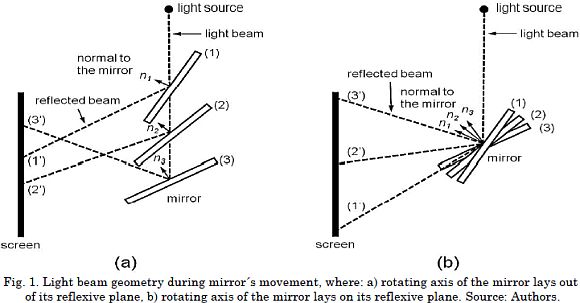
Scanning micromirror used in devices such as bar-cod readers, image projectors or tuned filters in spectrometers should provide suitable image quality. It means uniform optical resolution at each part of the image and as well lack of any distortion. Such conditions can be meet by a microscanner design in which the distance between reflective surface of the mirror and stationary source of light is constant. Let us consider two design cases presented in Fig. 1. In the first case, a mirror rotates around axis lying somewhere out of its surface (Fig. 1a). In the typical scanning micromirror design, actuators are connected directly to the mir-rors edge [3]. Here, the distance between mirrors surface and the source of light is variable and in return causes a non-uniform reflected light beams (1, 2 and 3) distribution. This results in irregular illumination of the screen.
In the second (Fig. 1b). Now, independently on the mirrors position, the light beam reaches the central point of the mirror, and reflected beams are distributed uniformly. In other words, reflected beam follows the mirrors position in linear manner. This in return causes homogenous illumination of the screen.
The main goal of the work was to propose such design of a scanning micromirror which meets following assumptions:
1. the mirror must be driven by thermobimorph actuators;
2. the mirror must tilt in one or two perpendicular directions;
3. the distance of the mirrors center from a stationary source of light must remain constant during full range of the mirrors movement.
Two designs of scanning micromirror have been proposed (Fig. 2) [4]-[7]. In the first one, the mirror is dedicated for 1D scanning (microscanner 1D), whereas in the second one, for 2D scanning (microscanner 2D). The microsanner 1D, Fig. 2a, is composed of a moving micromirror 1 suspended on two thermobimorhic beams 2 connected directly to a fix base 3. The beams play a rule of actuators tilting the mirror. In the proposed design, the mirrors rotation axis crosses the actuators in the middle and passes through the center of the mirror. Due to that, the center of the mirror keeps constant distance from the light source during the whole scanning action. The location of the scanners moving elements in respect to each other presents also reduced inertia and minimized influence of air damping. The latter two benefits enable higher both resonant and non-resonant frequencies of scanning movements of the mirror. Higher frequencies may increase the efficiency of optical switches, for example, but they may also enhance the quality of the projected image, which can be refreshed more often.
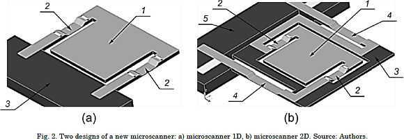
A microscanner 2D from the second design (Fig. 2b) is composed of a moving micromirror 1, four thermobimorphi beams and a rigid moving frame. The beams play a rule of actuators tilting the mirror, like in the first case. One pair of actuators, shorter ones 2, connects the mirror with the rigid frame 3. The second pair, longer actuators 4, situated perpendicular to the first one, connects the frame with a fixed base 5. Due to that, the mirror can rotate around two perpendicular axes lying in its plane. In both cases, as it has been already mentioned, thermobimorph beams have been used as actuators. Each beam is composed of two main layers which differ in coefficient of thermal expansion in proposed designs those are silicon and aluminum. Between the layers a resistive heater is placed. The heater has a form of meander line made of platinum. In order to insulate the heater from silicon and aluminum the heater is enclose in thin silicon dioxide layer.
2.2 Principle of operation
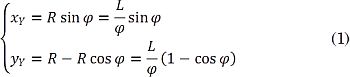
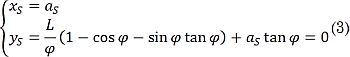
The following analysis proof that the distance between center of the mirror and a fixed source of light is nearly constant during the whole scanning action. Let us consider a mirror attached to one pair of actuator (Fig. 3a). Let the mirror and actuators lie initially in the plane y = 0. Then, the beginning and the end of the mirror take points A0 and B0 respectively, whereas its center - point C0. The actuators, of length L each one, are fixed at point X0 and attached to the mirror at point Y0. Hence, the distance between fixing point of the actuators and the center of the mirror is a0 and equal L/2. After fabrication process, when the structure is release, the actuators bend upward and incline the mirror to the substrate plane. Mentioned characteristic points A0, B0, C0, X0and Y0 move to points A, B, C, X = X0 and Y, respectively. Let us assume that deformation of actuators is affected only by internal stress which cause their pure bending. If so, the actuators take a form of arcs of circle of radius R and center at point O. The angle φ of the slope of the tangent to the actuators at the point Y in respect to the plane y = 0 describes the bend of the actuators and mirrors rotation.
Let us mark an intersection point of inclined mirror and axis x of the coordinating system {x, y} as S. Additionally, let as be the distance between point S and attachment point X = X0 and δ be the distance between point S and center point C of the tilted mirror. Due to symmetry in respect to line O-S the distance δC is same as between points C0 and S. During mirror movement, the value of δC changes together with the angle φ. Let δ yc be a distance between current position of the mirrors center C and the plane y = 0. Assuming 0 < φ=Π/2 the value of δ yc can be easily calculated
Coordinates of the movable end of each actuator can be expressed as a functions of angle φ:
Hence the tangent to the arc at point Y can be expressed by one of the two following equations:
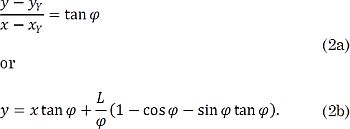
In that case, the point S which moves along the line y = 0 during mirror movement has coordinates:
From Equation (3):
Since δ yc (f)=aS (φ)-1/2 L, then
Where δ yc is the distance of point the C from plane y = 0. Based on Equation (5) it can be concluded that for angle φ ≤ 45°, the distance C is smaller than 2% of the length of actuators. Therefore, it can be stated that C0, C and S take the same position during mirrors movement. It means, that the center of the mirror is stationary despite rotation of the mirror, as it is depicted in Fig. 3b.
2.3 Design of microscanner 2D
The design of the microscanner was adapted to the available materials and technology of fabrication. In the final project, the mirror has square shape with edge length of 300 µm (Fig. 2b). The mirror is suspended on one pair of shorter actuators (66 µm), which allow for faster scanning direction at the frequency of about 1 kHz. To the other ends of actuators, a rigid, movable silicon frame is connected. Next, the frame is connected with a fixed base by one pair of longer actuators (220 µm). The longer actuators are responsible for slower – frame scanning direction at 60 Hz. The cross sections of both type of actuators are presented in Fig. 4.
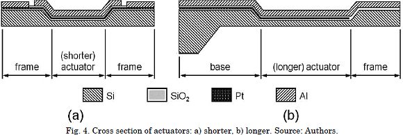
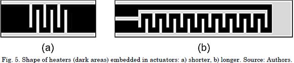
Heaters embedded in actuators have been designed as meander lines made of platinum (Fig. 5). Each heater is encapsulated between two layers of insulator (SiO2). One layer of SiO2 adheres to the passive layer (silicon) of actuator, whereas the second one to active layer (aluminum) of actuator.
3. Fabrication
3.1 Fabrication of microscanner on standard silicon wafer
Microfabrication of thermobimorph actuators itself is well known [8]. However, it is much more challenging to design appropriate microfabrication process to integrate monolithically the several actuators and mirror into one device. It must be noticed that in microfabrication, due to its nature, assembly is almost not possible, except for some particular cases. This makes both the design and the microfabrication more restricted.
Important part of the designing of fabrication process is to define the requirements to the substrate on which the device will be fabricated. It is important to pay attention to such wafer parameters like its crystallographic orientation, dopant type, resistivity, thickness and diameter, surface finish, etc. Another very important part of microfabrication is a set of photolithographic masks containing desirable patterns. The patterns are transferred to the substrate in photolithography processes.
The fabrication process is briefly depicted in Fig. 6. The process starts from anisotropic silicon etching. Firstly, the bottom surface of a silicon wafer is covered with photoresist and baked. Then, photore-sist is exposed to UV-light through the first mask. After exposure, the photoresist is developed (exposed areas are removed). In the next step the uncovered areas of SiO2 are etched, in that way opened areas allow for silicon etching in the next step. Unpro-tected silicon is etched by anisotropic wet etching in KOH solution. In results, thin (15 µm) membranes are obtained.
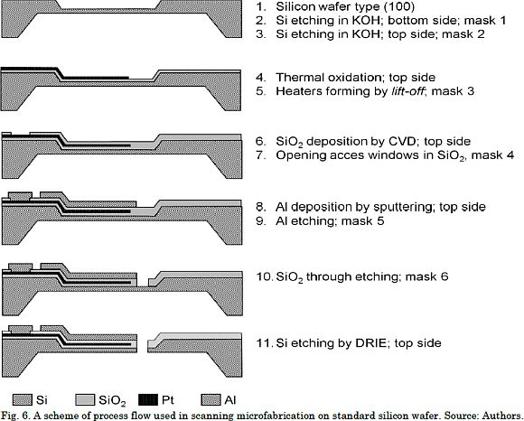
Performing subsequent photolithogra-phy with the use of the second mask fol-lowed by SiO2 wet etching, and then anisotropic silicon etching lead to obtain micromembrane with thickness of 3 µm. This photolithography is done on the top surface of the wafer. Such prepared wafer is next subjected to surface micromachining. By repeating processes of layer deposition, photolithography, and selective etching, different components of the microscanner are fabricated - conductive elements (heaters, electric paths), insulating layers, the frame, the mirror, etc.
Exceptional feature of the surface micromachining technique it its capability of fabrication of the structures of submicrometer thickness. Unfortunately, obtained layers suffer from residual stress. The sources of residual stress can be different, e.g. mismatch in the thermal expansion coefficients, nonuniform plastic deformation, lattice mismatch, substitutional or interstitial impurities, grow processes, etc.
During microscanner fabrication thermal oxidation of the wafer is applied. The process is used in order to obtain 100 nm thick insulating layer. Next, a film of 100 nm thick platinum layer is deposited by sputtering. However, in order to improve adhesion of platinum to the previously obtained thermal oxide, a layer of titanium must firstly be deposited. The thickness of titanium layer is just 20 nm. Since platinum is a noble metal, it is difficult to form structures of it by wet or dry etching.
Therefore, to form the heaters a lift-off method is applied. The method is relatively simple and very convenient for patterning thin films. Next, the heaters are covered by 100 nm thick SiO2 layer, but this time the insulating layer is deposited by CVD tech-nique. Finally, a 2.2 µm thick layer of aluminum is sputtered. To form active layer of actuators as well as electric paths and a reflective surface of the mirror, the aluminum layer is patterned by photolithography and wet etching. In order to obtain electrical contact between aluminum paths and platinum heaters firstly, windows in CVD silicon dioxide were etched before Al deposition. The last step of microfabrication was release the structures. This step was done by DRIE.
Since the fabrication process performed on SOI wafer does not differ significantly from the one performed on standard silicon wafer, only the important differences are described in the following chapter.
4. Results and discussion
4.1 Fabrication problems and obtained results on standard silicon wafer
The successful microfabrication depends strongly on the quality of the used materials. The process of fabrication on standard silicon wafer expose some difficulties. The biggest problem was to ensure uniform thickness of the membranes (3 µm) across the wafer.
One of the parameters describing quality of the wafer is total thickness variation (TTV). The wafer used for fabrication was characterized by TTV around 2 µm. Double side anisotropic wet etching of such wafer caused that in some places the wafer was etched through, where-as in others membranes had thickness of about 8 µm.
Two possible solutions of this problem could be to use wafers with much lower TTV parameter and optimize the etching process (e.g. temperature, stirring, etc.).
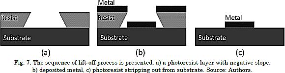
Another two difficulties in the microfabrication process were related to the photolithography step aiming to prepare the photoresist layer for heaters fabrication in lift-off process.
The sequence of lift-off process is presented in Fig. 7. Well prepared photoresist for metal lift-off process is characterized by negative slope of photoresist walls, or in other words the photoresist layer is undercut, Fig.7a. Such profile ensures discontinuity of deposited metal, Fig.7b. It is important to mention that the thickness of photoresist should be at least three times higher than deposited metal. To perform lift-off process, the substrate is immersed in a liquid made of a powerful photoresist solvent that is chemically inert on other layers. Once the dissolved photoresist is stripped out from substrate, the metal layer over it is lifted-off, while the metal deposited directly on the substrate remains. Remaining areas of metal form, the final heaters on the substrate, Fig.7c.
The problem which we have faced during lift-off process was that the process had to be done on membranes, on the bottom of 12 µm deep cavities. These implied difficulties with obtaining uniform photoresist layer by spin-coating and incorrect heaters´ shape projection on the membranes, Fig. 8.
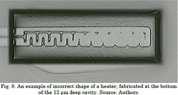
The photoresist layer with uniform thickness is easy to obtain on a flat surface. It is a compromise between process parameters such as acceleration, speed of rotation, spinning time and modification of photoresist viscosity. However, when the surface on which the spin coat-ing is performed has deep cavities or high structures protruding over the surface the spin coating becomes difficult to optimize. Therefore, another technique which allows to obtain constant photoresist film on non-flat surface is spray coating. The photoresist layer obtained by that technique is usually much thicker and it is characterized by grain-like structure. Thus, that technique is not convenient for lift-off processes where the resist thickness of 1-2 µm is preferable. However, working on deep cavities, spray coating may be the only possible solution to obtain uniform layer of photoresist.
Non-uniform photoresist thickness, but not only, had very strong influence on the above mentioned incorrect result of the heater fabrication. Another factor was excessively increased distance between the mask and the bottom of the membranes during UV exposure of the photoresist. In typical UV exposure, the mask is in direct contact with the substrate covered by photoresist or is separated from it of several micrometers or even a few tenths. The first one, called direct contact photolitography gives the best resolution down to 0.5 µm or better, whereas the second one, called proximity lithography, is affected by lower resolution ranging of 2-4 µm or more. The resolution depends directly on the separation the bigger separation the lower resolution and is simply a result of light diffraction on the edge of the pattern on the mask.
The possible solution of that problem could be modification of the pattern on the mask which takes into account diffraction phenomenon or to employ projection photolithography which use sophisticated optics. The first solution could be difficult to realize due to complicated pattern of the heater, whereas the second one would require specialized aligner, available typically in the industry, and would involve changes in the whole process of fabrication.
Fig. 9 In case of actuators, Fig.9a, such roughness has no significant influence on their work. Whereas, in case of the mirror, where the aluminum is dedicated to act as its reflective surface, Fig.9b. such drawback is a major problem. According to [9], optical scattering losses increase rapidly when roughness exceeds about 5% of wavelength, which for visible light corresponds to 20-30 nm. In that case, obtained roughness disqualifies the device from practical use.
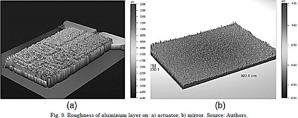
The problem of high roughness was reduced by increasing of deposition rate while absence of substrate heating.
The last issue appeared during structure releasing. In this step, the large cavities were etched by deep reactive ion etching (DRIE) method on the back side of the wafer. We found, that bottom side of the wafer is partially covered by thin film of silicon dioxide which probably remained not etched out completely after one of the previous processes. This forced longer etching time and in consequence caused that many structures were destroyed.
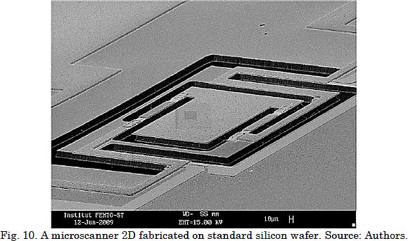
As a result, the presented process of microfabrication was finished with moderated success only on one from four processed standard silicon wafer. And only about 10% from fabricated structures were close to assumptions.
Their basic defect was too small tilt angles of the mirror in respect to the substrate plane, (Fig. 10). Designed thickness of passive layer was 3 µm, whereas the obtained one was about 8 µm, which means that it was slightly 2.7 times bigger than expected. Based on analysis of bim-etallic beam presented by Timoschenko in [10], one can show that the issue was caused by too thick passive layer of thermobimorphs. According to his theorem, the curvature of a bim-etallic beam is a function of thermo-mechanical properties (such as: modulus of elasticity, internal stress, thickness, coefficient of thermal expansion) of individual layers and temperature. Roughly, the curvature of the beam is inversely proportional to the square power of the passive layer thickness. So, for 2.7 times increase of the thickness causes more than 7 times decrees of the beam's curvature.
4.2 Fabrication problems and obtained results on SOI wafer
In order to improve quality of microscanners, SOI wafer has been used. This type of substrate is composed of three well defined layers: silicon, SiO2 and again silicon. Counting from top to bottom: the first silicon layer is called a, a device layer, SiO2 (an insulator layer) is called buried oxide (BOX), and the second silicon layer is called a handle layer. The thickness, crystallographic orientation as well as doping type of each silicon layer can be prepared on demand. For our purposes the SOI wafers were composed of 3 µm thick device layer, 100 nm thick buried oxide and 400 µm thick handle layer. Additionally, both sides of the substrates where covered with 100 nm thick thermal oxide. The device layer was dedicated for passive layer of the thermobimorph actuators.
As a consequence of employing SOI wafers, some modifications of fabrication process were required. Firstly, the number of masks has been reduced from 6 to 5. Wet etching was replaced by dry etching and shifted to the end of the process. Due to that, the other processes, especially photolithography steps, were performed on flat surfaces. Also, metal layers (platinum and aluminum) deposition have been modified.
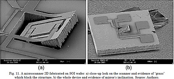
Introduced changes significantly reduced time of microfabrication and improved quality of the fabricated structures. Unfortunately, some new difficulties appeared: bad adhesion of the second SiO2 layer to platinum and problems with deep etching of handle layer. Non-uniform silicon thickness which looked like grass (called just grass or black silicon) caused that released structure were blocked (Fig. 11a). There could be two reasons that black silicon appeared: one - some contaminations on the etched surface remained after previous process, two - re-deposition of etching products. In both cases microscopic particles act like micromasks causing reduced etch rate or they can even stop the etch process.
From the other side, due to well defined device layer, from which the actuators were made of, the plane of the mirror tilted significantly out of plane as expected, Fig. 11b.
5. Conclusion
Some problems related to the fabrication of MEMS, on the example of the microscanner device, have been shown. The device may be used for laser beam scanning applications. The device consists of a micromirror which is displays in one or two directions by two or four electrothermal actuators, respectively. The actuators have a form of bimorph cantilever beams. A special location of the mirror with respect to the cantilever beams assures a high precision of the scanning action. Namely, the distance of the center of the mirror from the light source is the same during the scanning process. Moreover, the inertial moments of movable parts, as well as influence of air damping are minimized. It allows to obtain a higher resonant frequency for scanning, and hence, more smooth projected image. Moreover, a more precise motion of the mirror causes less distortions of the image. It is necessary to point out, that the fabrication process of the device is very simple and compatible with IC technique.
The device was fabricated in two versions: as a scanner with one degree of freedom and as a scanner with two degrees of freedom. To perform its prototypes, a fivemask micromashing process has been used. For the production, the standard materials (silicon, silicon dioxide, platinum, aluminum), and typical techniques have been applied.
The process was repeated twice using two different types of substrate: a standard silicon wafer and a SOI substrate. The technique based on the standard silicon wafer has created many problems. It has appeared that only 10% from fabricated structures were close to assumptions. The basic defect of fabricated structures was too small tilt angles of the mirror in respect to the substrate plane. Numerous attempts have shown that changing the silicon substrate to the SOI-type has reduced the microfabrication time and it has improved the quality of the structures. Concluding, the SOI-type substrate gives much better results and it is preferable to manufacture this type of MEMS devices.
6. Acknowledgments
The work presented in the article has been performed in FEMTO-ST Institute in Besançon, France in the team of prof. Christophe Gorecki. Authors acknowledge the French RENATECH network through its FEMTO-ST technological facilities MIMENTO.
References
[1] P. R. Patterson, D. Hah, M. Fujino, W. Piyawattanametha and M. C. Wu, “Scanning micromirrors: An overview”, In: Optics East. International Society for Optics and Photonics, 2004. pp. 195-207. [ Links ]
[2] E. Pengwang, K. Rabenorosoa, M. Rakotondrabe and N. Andreff, “Scanning micromirror platform based on MEMS technology for medical application”;, in Micromachines, 7, 2, 24. [ Links ]
[3] G. Lammel, S. Schweizer and P. Renaud, “Optical Microscanners and Microspectrometers using Thermal Bimorph Actuators”, Boston: Kluwer Academic Publishers, 2002. [ Links ]
[4] W. Gambin and A. Zarzycki, “Urzadzenie skanujace”. PL Patent 216517 (B1), 30 April 2014. [ Links ]
[5] W. Gambin and A. Zarzycki, “Thermal and dynamical analysis of a new microscanner behaviour,” in Proc. of the 1-st Int. Conf. Multidisciplinary Design Optimisation and Application, Besancon, 2007. [ Links ]
[6] A. Zarzycki and W. Gambin, “New thermally actuated microscanner-design, analysis and simulations,” in Recent Advances in Mechatronics, Berlin, Springer, 2007, pp. 526 - 530. [ Links ]
[7] W. Gambin and A. Zarzycki, “Optimal design and analysis of a new thermally actuated microscanner of high precision,” Int. J. Simul. Multidisci. Des. Optim., vol. 2, pp. 199 - 208, 2008. [ Links ]
[8] M. Madou, Fundamentals of Microfabrication, Boca Raton: CRC Press, 2002. [ Links ]
[9] S. Franssila, Introduction to Microfabrication, John Wiley & Sons, 2010. [ Links ]
[10] S. Timoshenko, “Analysis of Bi-metal Thermostats”, J. Opt. Soc. Am., 11, pp. 233-255, 1925. [ Links ]

